The Scenic Route to Repairing a Self-Destructing SRS DG535 Digital Delay Generator
- Introduction
- The Stanford Research Systems DG535
- Who Uses a Pulse Delay Generator?
- Inside the DG535
- The Annoying Mechanical Design of the DG535
- It’s Always the Power Supply
- Power Architecture of the DG535
- The How, Why, and Please Don’t of Current Boost Resistor Circuits
- Root Causing the DG535 Issue
- Debugging the +7V Issue
- Side Quest: Debugging the CPU System - Connector Stupidity
- Fixing the Burnt PCB Trace
- Endless Boot Loop after Reassembly
- DG535 Up and Running with a Variac
- Tracking down the +12/-12V on the +9/-9V Rails
- LCD Replacement
- Post Mortem
- References
- Footnotes
Introduction
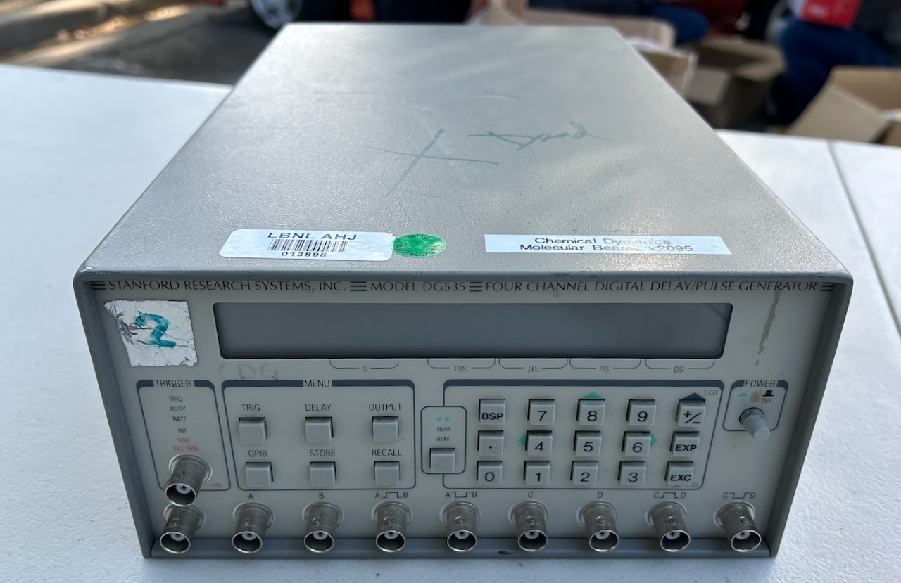
I got my hands on a Stanford Research Systems DG535 at the Silicon Valley Electronics Flea Market, $40 for a device that was marked “X Dead”.
That’s a really good deal: SRS products are pricey and even the cheapest Parts-Only listings on eBay are $750 and up. Worst case, I’d get a few weekends of unsuccessful repair entertainment out of it, but even then I’d probably be able to recoup my money by selling pieces for parts.1 Just the keyboard PCB is currently selling for $1502.
It doesn’t matter how broken they are, the first step after acquiring a new toy is cleaning up years of accumulated asset tracking labels, coffee stains, finger grime and glue residue. This one cleaned up nicely; the front panel is pretty much flawless:
After an initial failed magic smoke repair attempt, the unit went back to the garage for 18 months, but last week I finally got around to giving it the attention it deserves.
The repair was successful, and when you only look at the end result, it was a straightforward replacement of a diode bridge and LCD panel. However, the road to get there was long and winding. The broken power architecture and awkward mechanical design of the SRS DG535 made it way too easy to damage the device because I was trying to repair it.
So let’s get this advise out of the way first:
Do NOT power on the device with the analog PCB disconnected. It will almost certainly self-destruct with burnt PCB traces.
The details will be explained further below.
The Stanford Research Systems DG535
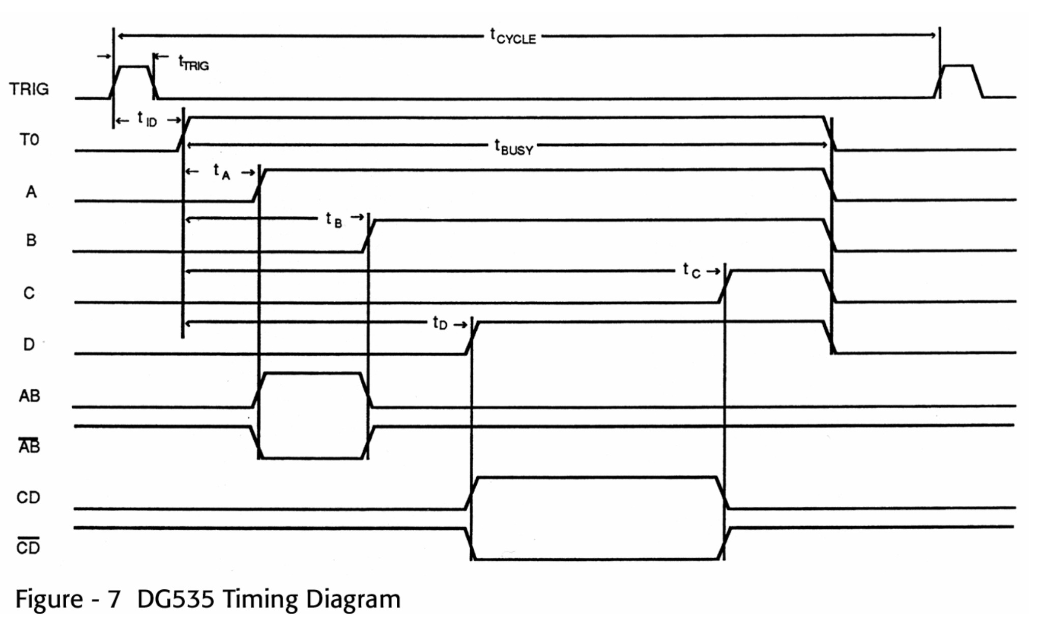
Conceptually, the purpose of the DG535 is straightforward: it’s a tool that takes in an input trigger pulse and generates 4 output pulses after some programmable delay. What makes things interesting is that these delays can be specified with a 5 ps precision, though the jitter on the outputs far exceed that number.
The DG535 has 9 outputs on the front panel:
- T0 marks the start of a timing interval. You’ll most likely use it when you use the device with an internal trigger to know when a timing sequence has started. There is delay of around 85ns between the external trigger and T0.
- 4 channels A, B, C and D can independently be configured to change a programmable time after T0 or after some of the other channels.
- Output AB is a pulse for the interval between the time set for A and B. It’s an XNOR between those 2 channels. -AB is the inverse of output AB. CD and -CD are the same for channels C and D.
 (Click to enlarge)
All outputs support a number of logic standards: TTL, ECL, NIM3, or fully programmable voltage amplitude and offset.
Settings can be entered through the front panel or through a GPIB interface that is available at the back of the device.
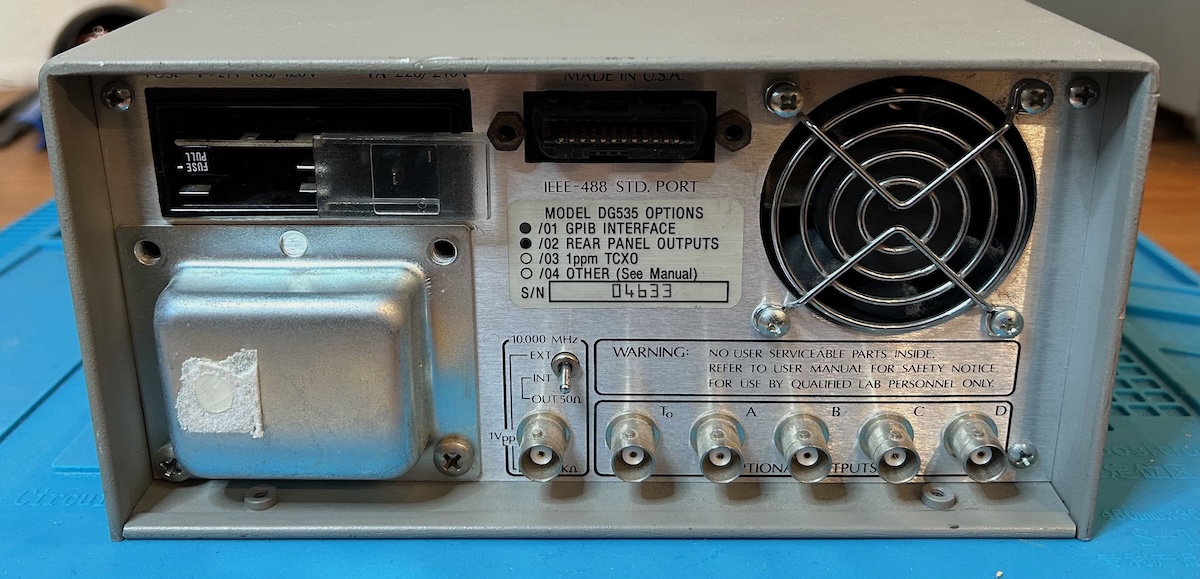
In addition to the GPIB interface, the back has another set of T0/A/B/C/D outputs because my unit is equiped option 02. These outputs are not an identical copy of the ones in the front: their amplitudes can go from -32V to 32V when terminated by a 50 Ohm impedance and each output has pulse width of roughly 1 us.
There is also a connector and a switch to select either the internal or an external 10 MHz timebase. Missing screws around the transformer housing are an indication that I’m not the first one who has been inside to repair the unit.
This 1993 ad lists the DG535 for $3500. It is currently still for sale on the SRS website for $4495, remarkable for an instrument that dates from the mid 1980s. I assume that today’s buyers are primarily those who need an exact replacement for an existing, certified setup, because the DG645, SRS’s more modern successor with better features and specs, costs only $500 more.
Who Uses a Pulse Delay Generator?
Anyone who has a setup where multiple pieces of test or lab equipment need to work together with a strictly timed sequence.
When you google for applications where the DG535 is used, you get a long list of PhD theses, national or military laboratory documents, optical setups with lasers and so on. Look closer at the first picture of this blog post and you can see that mine was used by Chemical Dynamics in a molecular beam setup… whatever that is.
Here are just a few examples:
-
We employed a delay generator (SRS system, DG535) to control the timing of the plasma and measurement systems. The DG535 generator was externally triggered by the pre-triggering signal from the laser system and then sent sequential TTL signals to trigger the ns pulse generator and camera.
-
Astigmatism-free 3D Optical Tweezer Control for Rapid Atom Rearrangement
Images were taken at delayed time steps (250-ns shutter, SRS DG535) as the translation stage was stepped from Z min = − 24.5 mm to Z max = 24.5 mm.
-
A delay generator (SRS DG-535) synchronized the laser and detection systems to capture time-integrated spectra at each point.
-
High-precision Gravity Measurements Using Atom-Interferometry
The timing of the pulsesis controlled by a set of synchronized pulse generators (SRS DG535), one of which also triggers all the hardware involved in generating the Raman frequencies.
-
Physics of Plasmas - Laboratory generation of multiple periodic arrays of Alfvénic vortices
Each antenna was switched on with a pulse generator (Stanford SRS-DG535), which then activated two arbitrary waveform generators (Agilent 3322A).
-
Liquid-to-gas transfer of sodium in a liquid cathode glow discharge
The laser system, operating at a 200 Hz repetition rate, was synchronized with the plasma discharge using a SRS DG535 delay generator, allowing time-resolved measurements of Na fluorescence during and after the discharge pulse.
At this time, I don’t have a use for a pulse delay generator, but as a hobbyist it’s important to keep the following in mind:
We buy test equipment NOT because we need it, but because one day we might need it.
I don’t see a future where I’ll be doing high-precision gravity measurements in my garage, but a DG535 could be useful to precisely time a voltage glitching pulse when trying to break the security of a microcontroller, for example.
Inside the DG535
It’s not complicated to create pulse delay generator as long as delay precision and jitter requirements are larger than the clock period of the internal digital logic: a simple digital counter will do. But when the timing precision is smaller than the clock period, you need some analog wizardry to make it happen.
SRS includes detailed schematics and theory of operation for many of their products and the DG535 is no exception. It’s a great way to study and learn how non-trivial problems were solved 40 years ago.
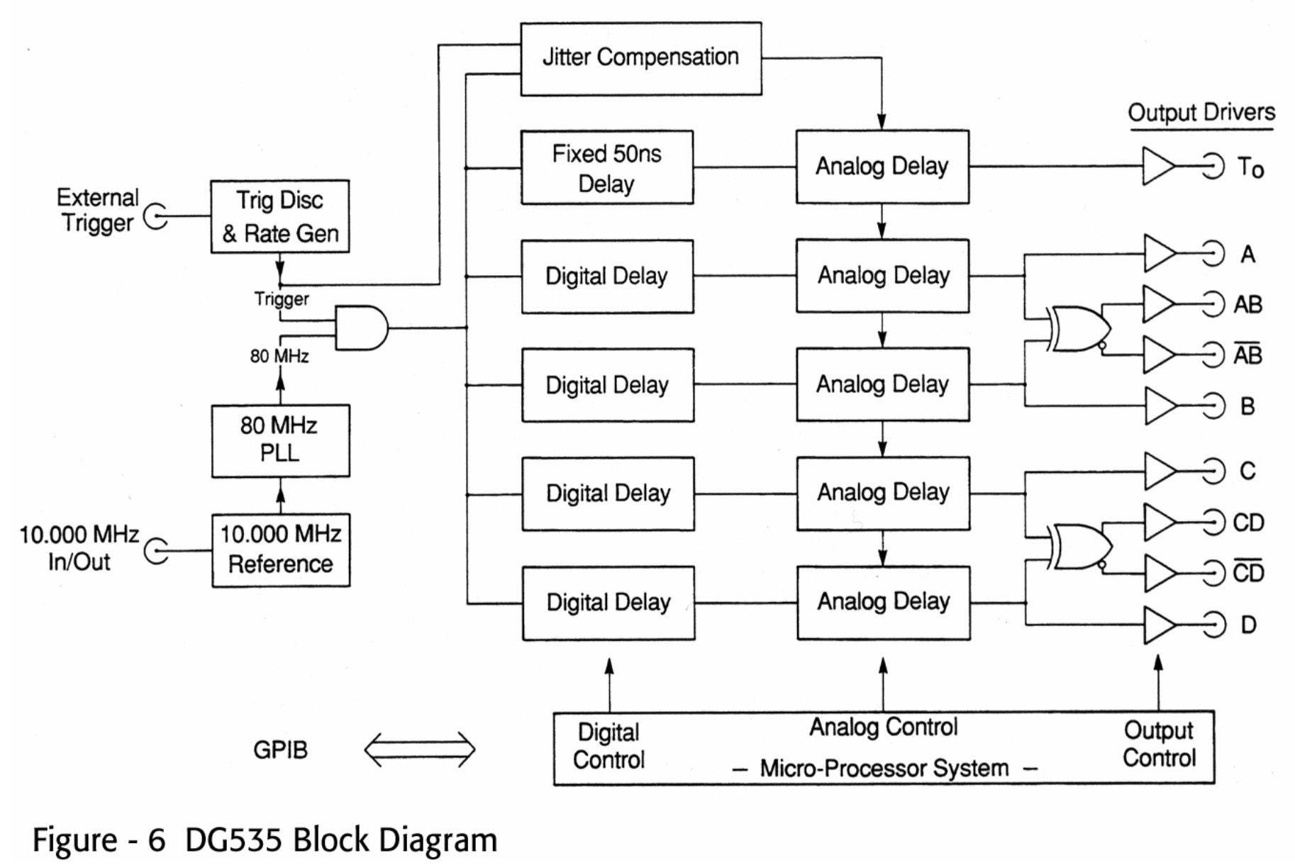
The DG535 takes a combined digital/analog approach to create delays of up to 1000 s. With an 80 MHz internal clock, the digital delay can be specified with 12.5 ns of precision. The remainder is handled by two analog circuits: the jitter circuit measures the delay between the start of the external trigger and the next rising edge of the 80 MHz clock. The analog delay circuit creates a delay between 0 and 12.5 ns after digital delay has expired. Channels A/B/C/D each have their own instance of the analog delay circuit.
 (Click to enlarge)
I will leave the low level details to a future blog post, but at their core, both the jitter and analog delay circuit work by precharging and discharging a capacitor with a constant current source for a time that varies between 0 and 12.5 ns. Precharging the analog delay capacitor is controlled by a 12-bit DAC. If you were wondering where the 5 ps of precision limit is coming from: 12.5 ns / (2^12) = 3 ps. Close enough!
Using a capacitor to measure time with higher precision that the digital clock is called “analog interpolation”. It’s often used by time interval and frequency counters such as the SRS SR620. I briefly touch this in my blog post about linear regression in frequency counters.
The Annoying Mechanical Design of the DG535
In my blog post about the SR620, I comment on a mechanical design that gives full access to all components by just removing the top and bottom cover. The DG535 is a different story.
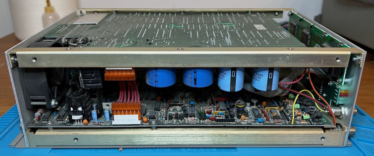
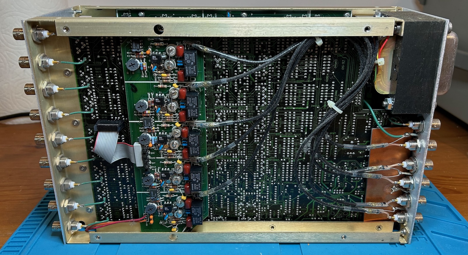
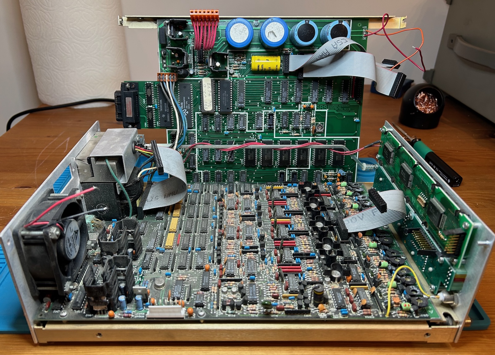
While the covers are just as easy to remove, the functionality is spread over 2 large PCBs, mounted with components facing inwards, and connected with a bunch of cables that are too short to allow separating the PCBs.
 (Click to enlarge)
 (Click to enlarge)
SRS was clearly aware that this PCB arrangement makes the unit harder to repair, because they helpfully added component designators and even component name annotations on the solder side of the PCB, though, sadly, there are no dots to mark pin 1 of an IC.4
Most cables have connectors and can easily unplugged, but not all of them.
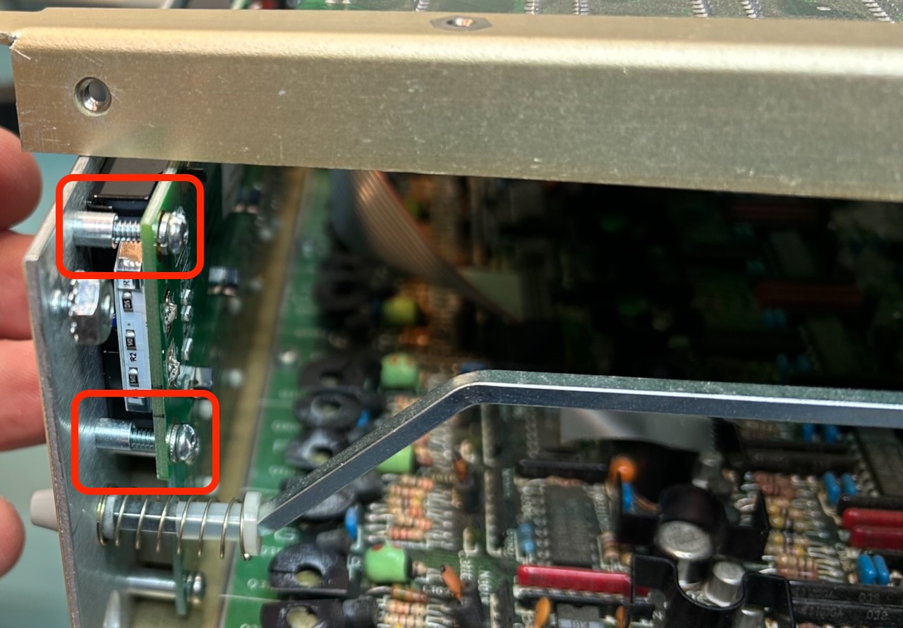
The red and orange wires in the picture above deliver +20 and -20V from the top PCB to the OPT02 PCB that is mounted below the bottom PCB. They are just long enough. If you want to take the unit apart, your only choice is desoldering these wires. It’s not rocket science, but… really? You also need to desolder the wires that power the cooling fan.
Enough whining… for now. When all wires are desoldered, connectors disconnected and screws removed, you can fold open the top PCB from the rest of the unit and get a full view of the inner components:
 (Click to enlarge)
We can see:
- a top PCB that contains a Z80-based controller and the counters that are used for the digital delay generation
- a bottom PCB with the rest of the delay and output driver circuitry
- the front has a generic LCD panel and a keyboard and LED PCB
It’s Always the Power Supply
Before taking it apart, I had already powered up the device and nothing happened: the LEDs and the LCD screen were dead, only the fan spun up. No matter what state a device is in, you always have to make sure first that power rails are functional.
The power architecture is split between the top and bottom PCB, but the two secondary windings of the power transformer first go to the top PCB. Since the transformer is located at the bottom, you always need to keep top and bottom PCBs closely together if you want to make live measurements.
 (Click to enlarge)
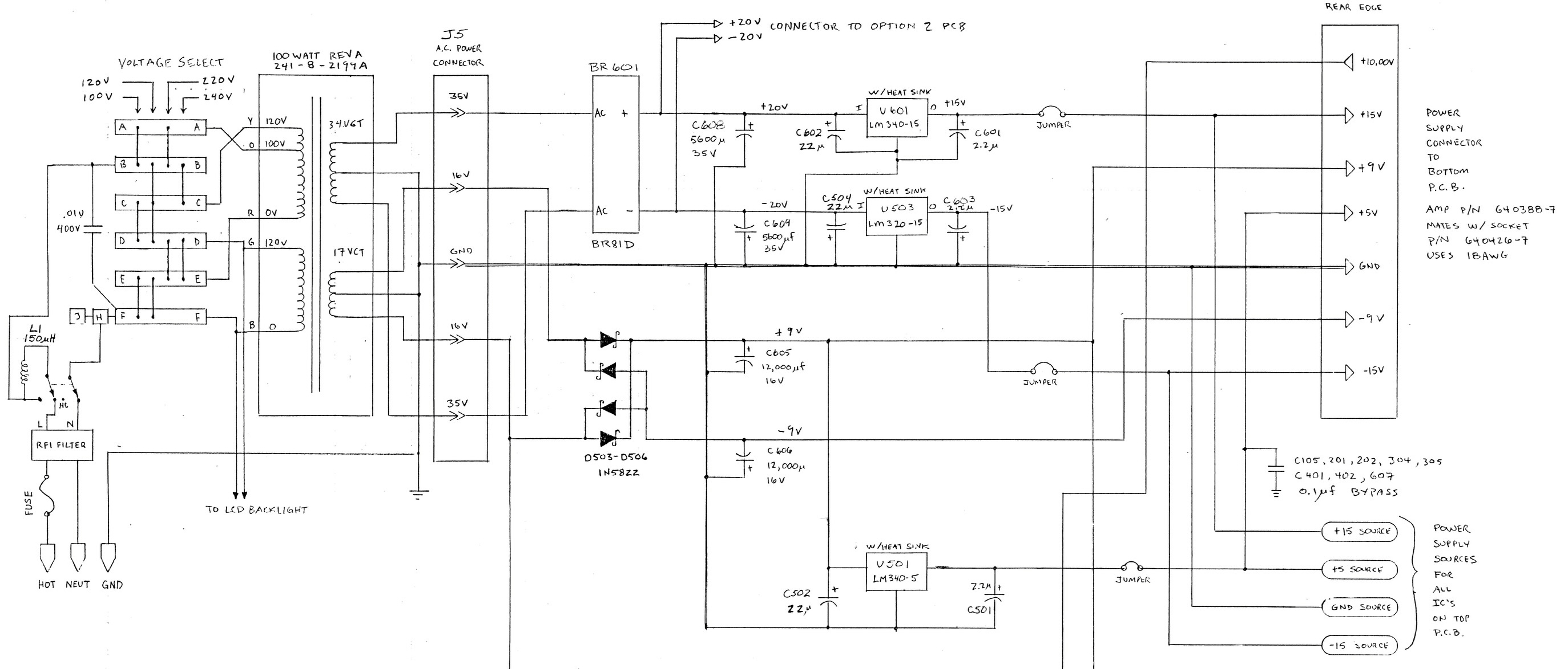
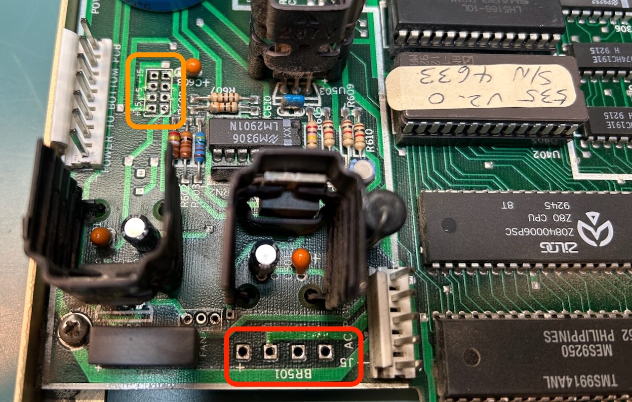
On the schematic, we can see the output of integrated full-bridge rectifier BR601 go to linear regulators U601 and U503 to create +15V and -15V and then immediately to the connector on the right which goes to the bottom PCB. These voltage rails are not used by the top PCB.
A discrete diode bridge and some capacitors create an unregulated +/-9V that goes to the same connector and to U501 / LM340-5, a linear +5V regulator that is functionally equivalent to a 7805. The 5V is used to power pretty much the entire top PCB as well as some ICs on the bottom.
I measured the following voltages on the top-to-bottom power connector:
- 0V - instead of 10V
- +15V - good!
- +12V - instead of +9V
- +7V - instead of +5V. Horrible!
- GND
- 0V - instead of -9V
- -15V - good!
The lack of 10V is easy to explain: it’s an input, generated by a high precision voltage reference on the bottom PCB out of the +15V. On the top PCB, it’s only used for dying gasp5 and power-on/off reset generation.
+12V instead of +9V was only a little bit concerning, at the time. The lack of -9V was clearly a problem. And applying +7V instead of +5V to all digital logic is a great way to destroy all digital logic ICs.
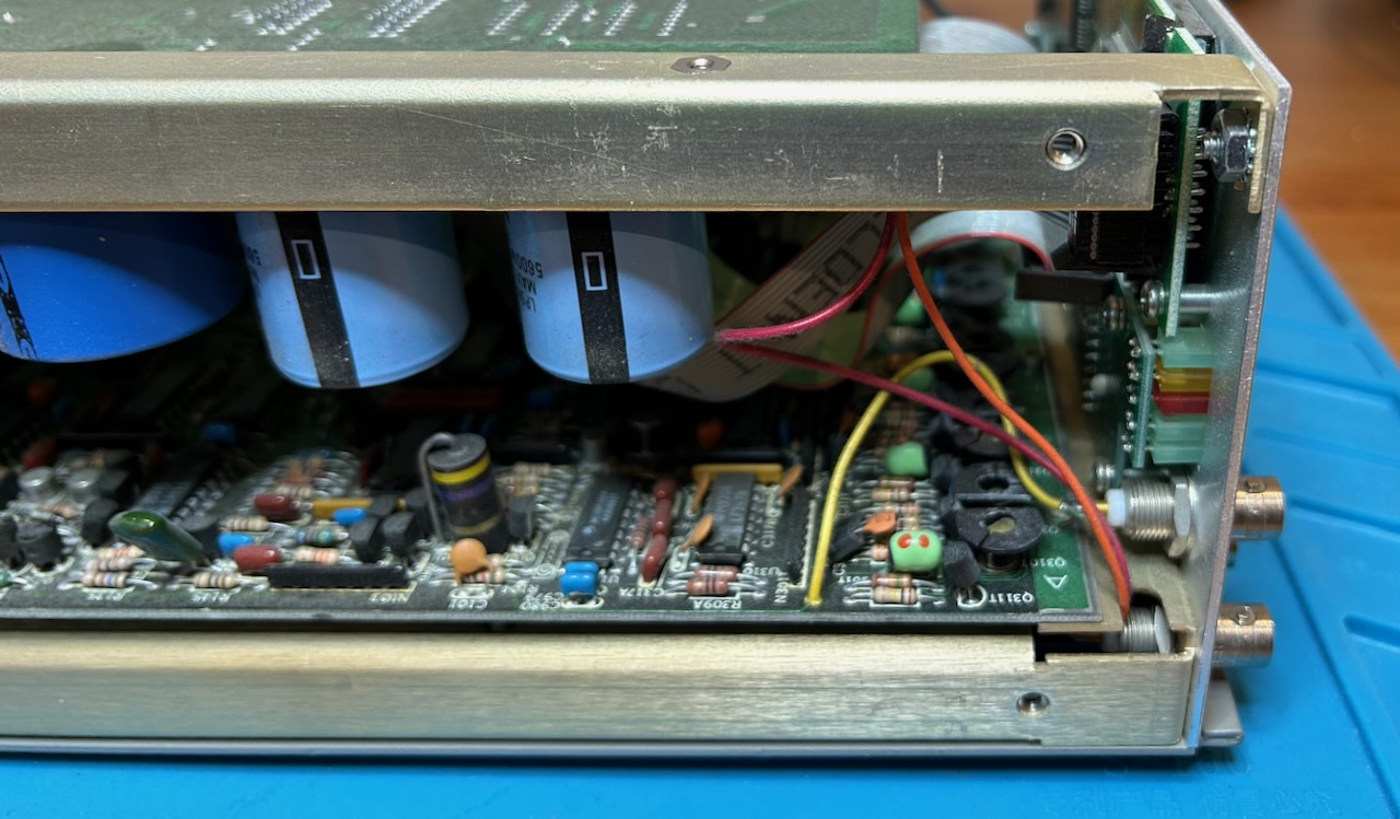
Here’s the part of the PCB with the 9V diode bridge:
Observations:
- the discrete diodes look like a bodge
- marked in red, there is a blackened spot above-right of the diodes
- there is a green patch wire. There are quite a bit of those on the top PCB and they turned out to be harmless; they work around bugs in the PCB itself.
2 discrete diodes were on the other side of the PCB to complete the discrete full bridge, though one soon fell off. Underneath the discrete diodes is a footprint for a BR501 full bridge rectifier that is not in the schematic6!
While doing these measurements, magic smoke appeared at the same location as blackened spot in the picture. At that point, I called it quits and left the unit sit for 18 months.
The schematic shows jumpers on the +/-15V and the +5V rail, see the orange rectangle in the previous picture. These are intended for power measurements, but when removed they also disconnect the not-at-all-5V rail from the digital logic and thus protect it from further damage until I had sorted out the issue.
Power Architecture of the DG535
Since I suspected a problem with the discrete diode bridge bodge on the top PCB, the plan was to repopulate the PCB with an integrated full-bridge rectifier. Turns out: even though the schematic in the manual shows a discrete bridge, the schematic description in the same manual indeed talks about an integrated full bridge. Instead of buying one at Digikey and pay $7 for shipping a $1 component, I found a suitable 100V/2A alternative, a 2KBP01M, at Anchor Electronics, the last remaining Silicon Valley retail components supplier, conveniently located across the street from work.
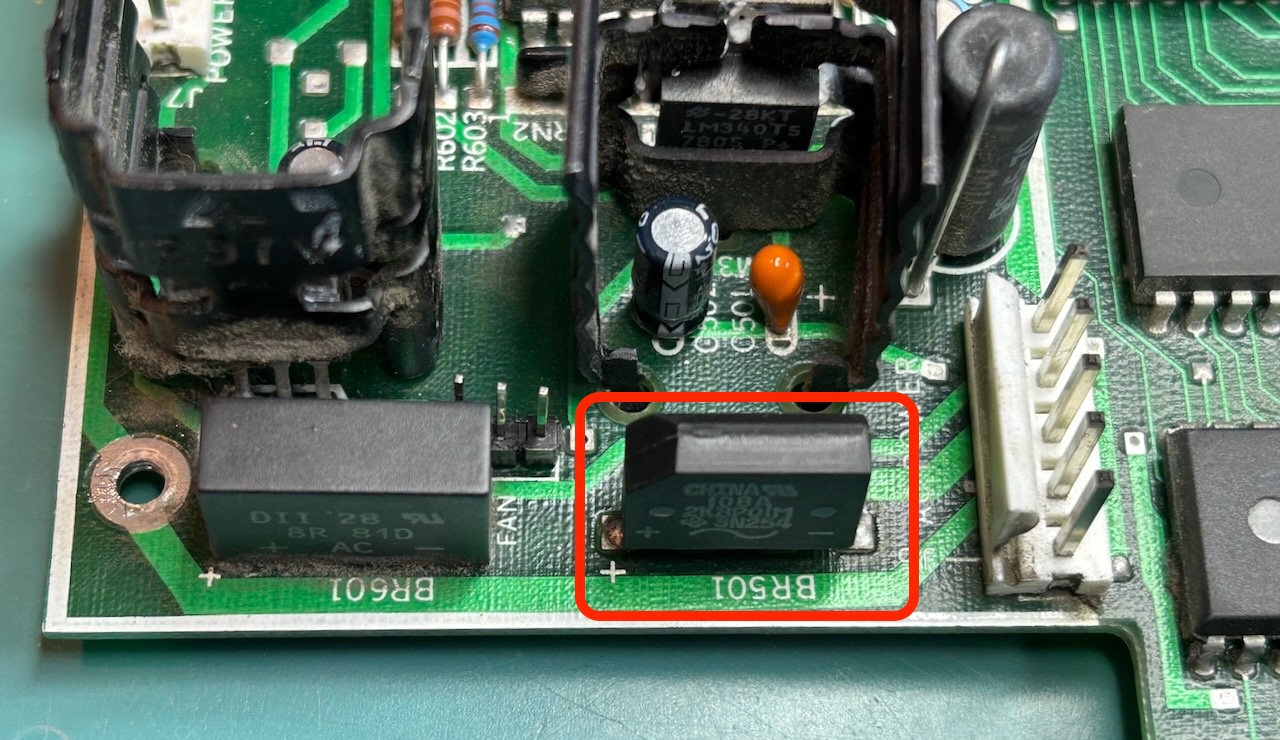
The footprint of the new diode bridge wasn’t quite the same, but you can easily nudge the pins a bit to make it work.
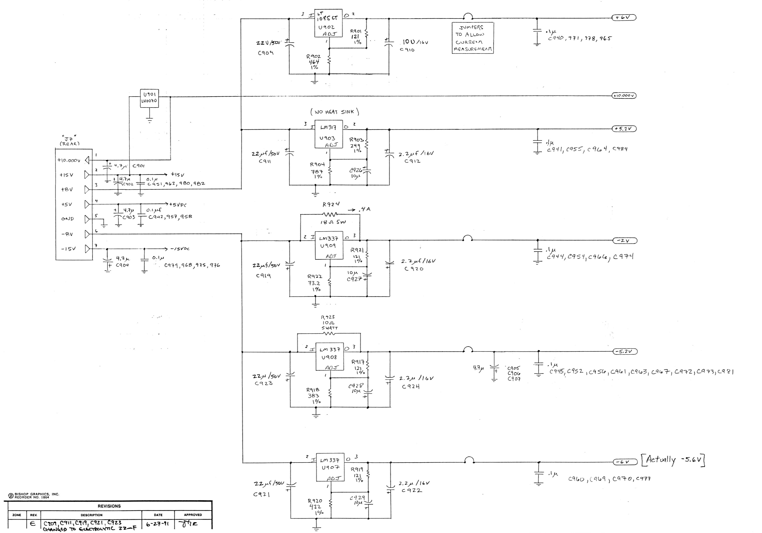
I then had a look at the schematic of the bottom PCB power supply:
 (Click to enlarge)
More linear regulators, 2 on the unregulated +8V (?) rail to create +6V and +5.2V, and 3 on the unregulated -8V rail to create -2V, -5.2V, and -6V (“actually -5.6V”).
Now here’s the interesting part: the -2V and -5.2V rails have heavy duty 5W 18 Ohm and 10 Ohm resistors between the input and the output of their linear regulator.
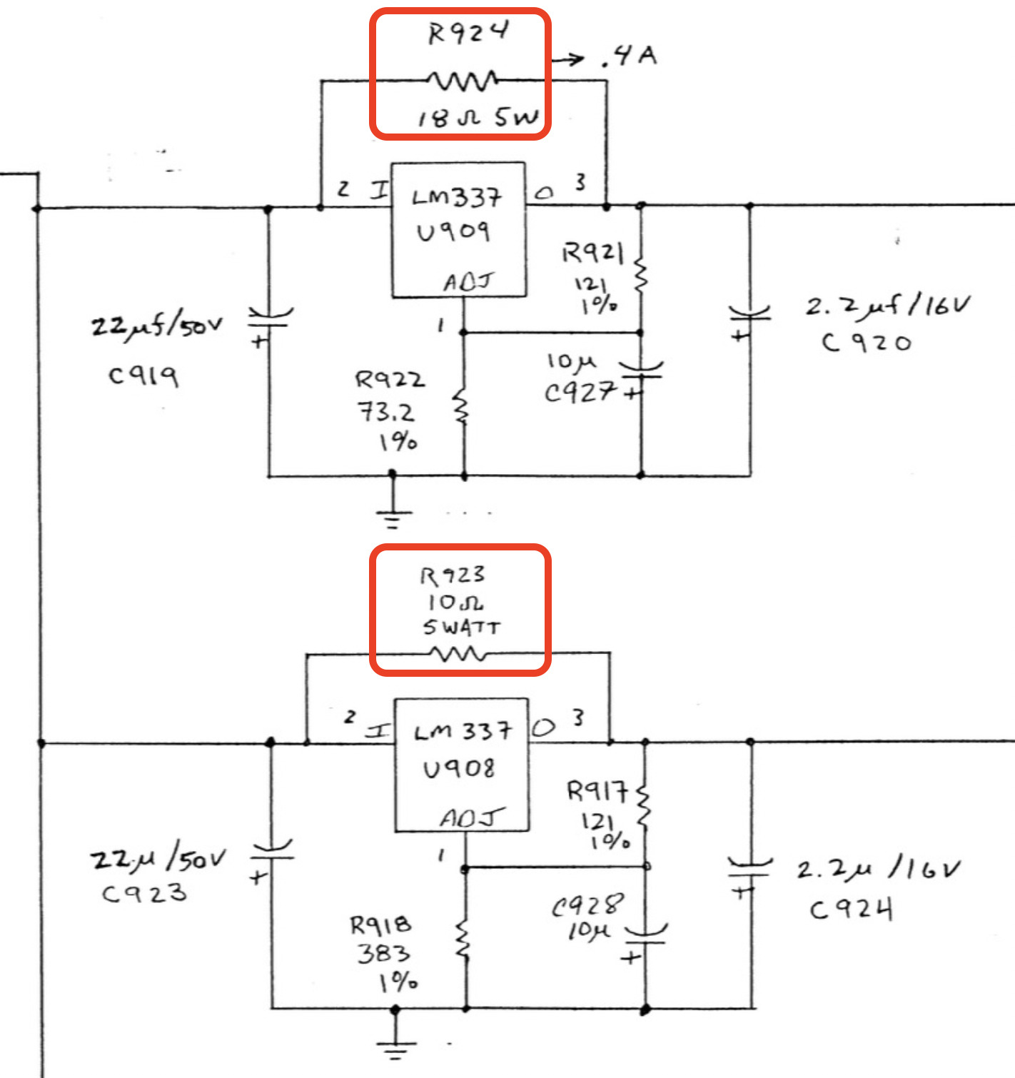
These are called current boost resistors and while they are useful in the right conditions, they are bad news. And when we go back to the top PCB, here’s what we see:
It may not be in the schematic, but located below right next to the 5V regulator is another 10 Ohm 5W current boost resistor.
The How, Why, and Please Don’t of Current Boost Resistor Circuits
The purpose of a current boost resistor is to partially offload a linear regulator.
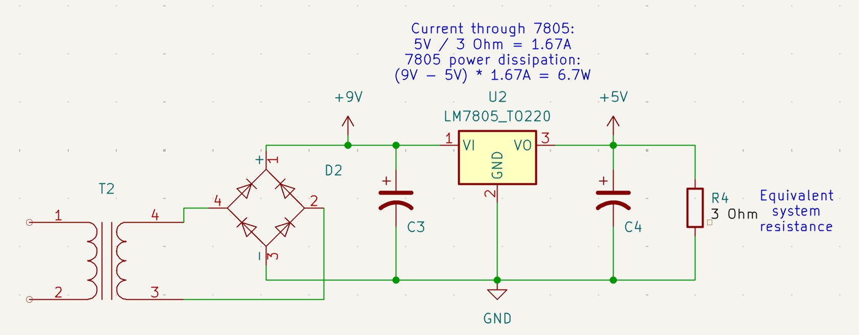
Imagine we have design with a 5V rail and a load with an equivalent resistance of 3 Ohm, good for a constant current draw of 1.67A. When we only use a linear regulator with 9V on the input side, the current through the regulator will be 1.67A as well and the regulator needs to dissipate (9-5) * 1.67 = 6.7 W. That is too much for a 7805 in TO-220 package to handle: with the right heatsink, 1.5A is about the limit.
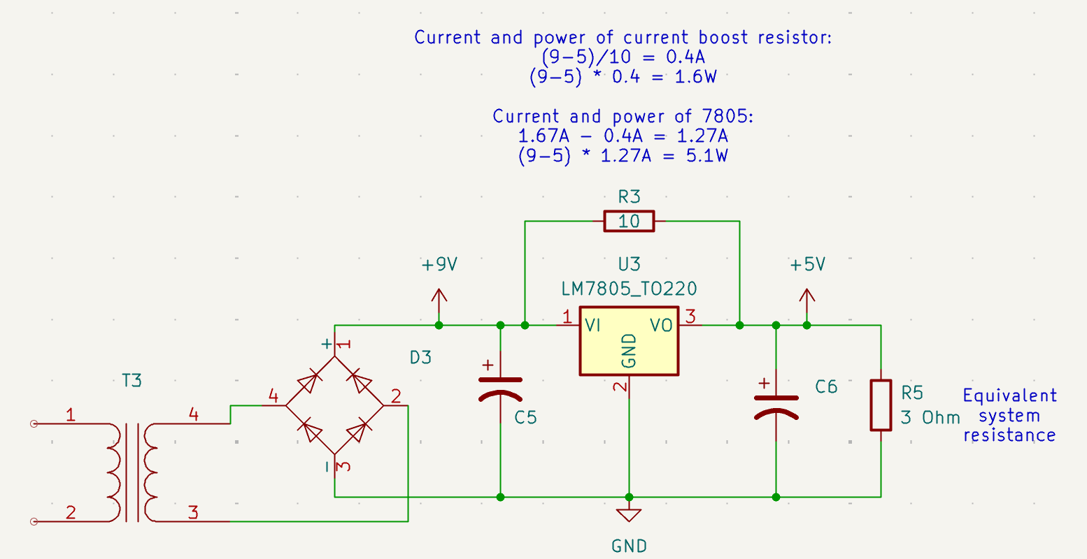
With a 10 Ohm current boost resistor, the 7805 still supplies current to keep the voltage across the load at 5V, but the current boost resistor injects a constant current of (9-5)/10 = 0.4A. This reduces the current through the regulator from 1.67 A to 1.27 A and its power dissipation from 6.7W to 5.1W. The dissipation in the resistor is (9-5)^2 / 10 = 1.6 W. The total power consumption remains the same: 5.1 W + 1.6 W = 6.7 W.
What have we gained? For the price of adding a beefy 10 Ohm resistor, we’re now staying within the current and power limits of the 7805 in TO-220 package. There is no need to upgrade the 7805 to a much larger TO-3 package and the changes to the PCB are minimal.
But there is a price to pay! In fact, there’s more than one.
Overvoltage risk when system load goes down
A linear regulator can only supply current from input to output; it can’t sink current from output to input. If the system load drops below the 0.4A that’s supposed to be supplied by the current boost resistor, that 0.4A has nowhere to go and the voltage at the output of the regulator has to go up.
We can see that here:
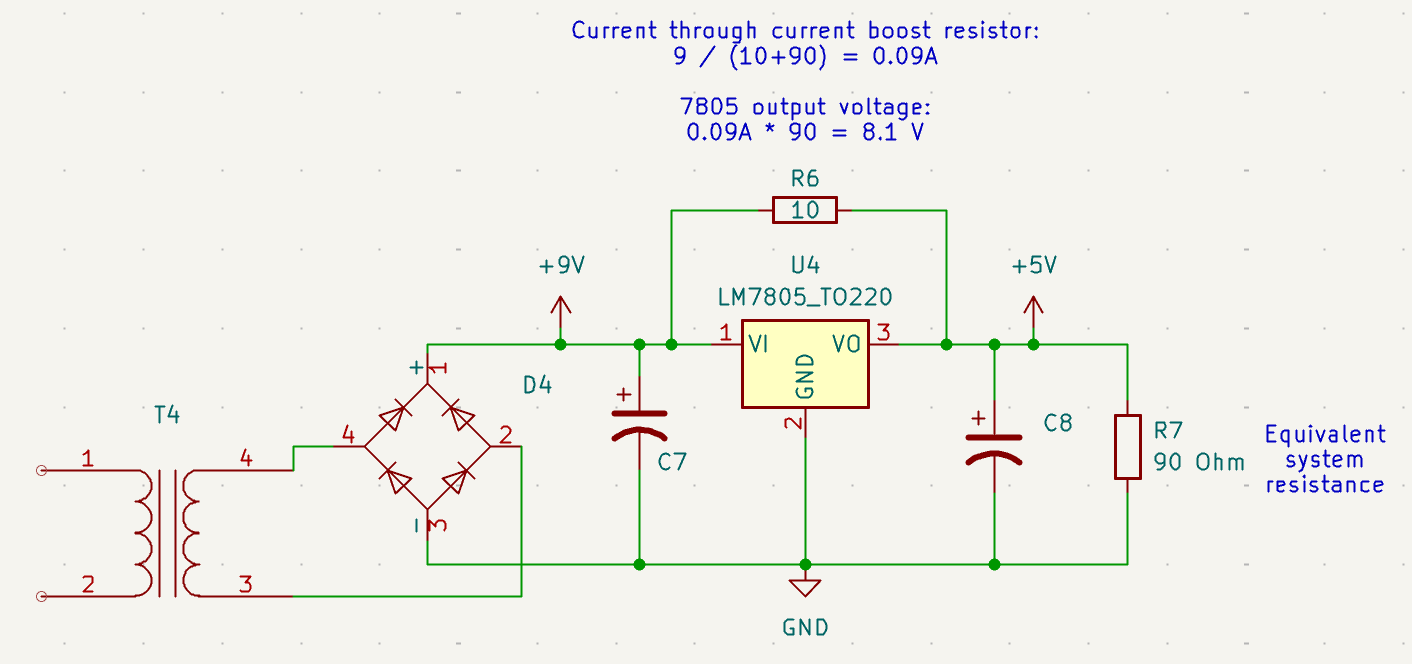
Assume that the system load has reduced and the equivalent system resistance is now 90 Ohm instead of 3 Ohm. The current through the 2 resistors is just 0.09A. The voltage at the 7805 output node is 8.1V and there is nothing the 7805 can do to bring the voltage down.
No safeguards when input voltage goes up
Another issue is when the input voltage increases. In the example below, it goes from +9V to +12V. The power dissipation in the 7805 goes up a little bit, but the one in the current boost resistor increases from 1.6W to 4.9W.
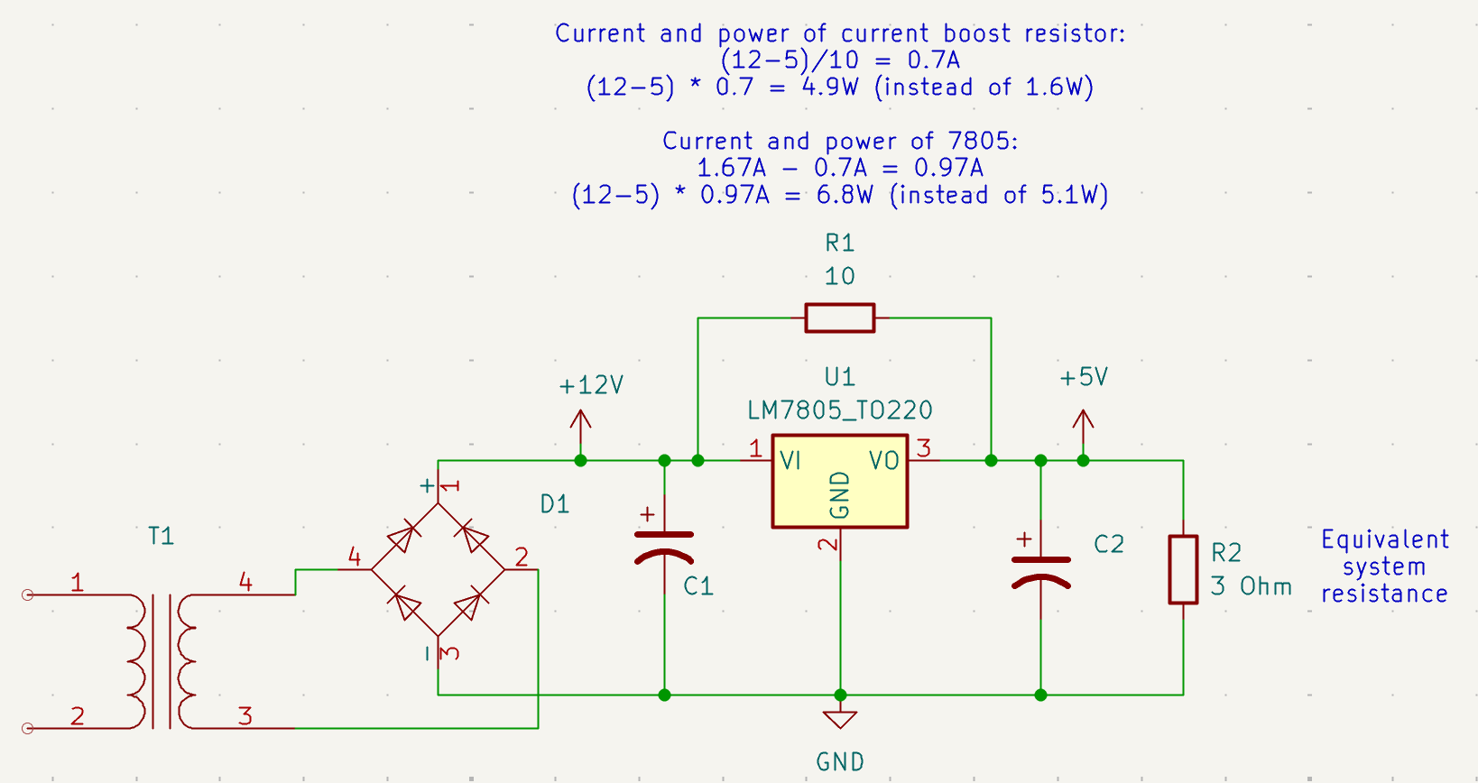
The +12V that I measured on one of the connector is more than just a little bit concerning after all.
Even without the current boost resistor, +12V at the input would be a real problem, since all the power of the resistor would have to be dissipated by the regulator. But with only a regulator, there is at least the possibility of including safeguards: there could be a current limiter, a temperature monitor, worst case, the regulator burns out and disconnects the output from the input. With a dumb resistor you have none of that.
In my 5370A repair blog post, I describe the current limiters that are part of its discrete linear voltage regulators: when the current is too high, the output voltage is reduced. The DG535 has no such safety mechanism.
Root Causing the DG535 Issue
Let’s recap the issues that I had to deal with:
- +7V on the +5V rail
- +12V instead of +9V at the input of the 7805 regulator
- A blackened PCB
These issues were all related.
Debugging the +7V Issue
The +7V could be explained by the current boost resistor and a load that was too low. If the load is too low anyway, why not temporarily desolder the current boost resistor and check what happens? I did that and the voltage on the +5V rail predicably dropped down to +5V. The temperature on the 7805 remained in check. Good!
But why was the load too low?
A quick probe on the pins of the Z80 CPU showed no activity. Better yet: there was no clock!
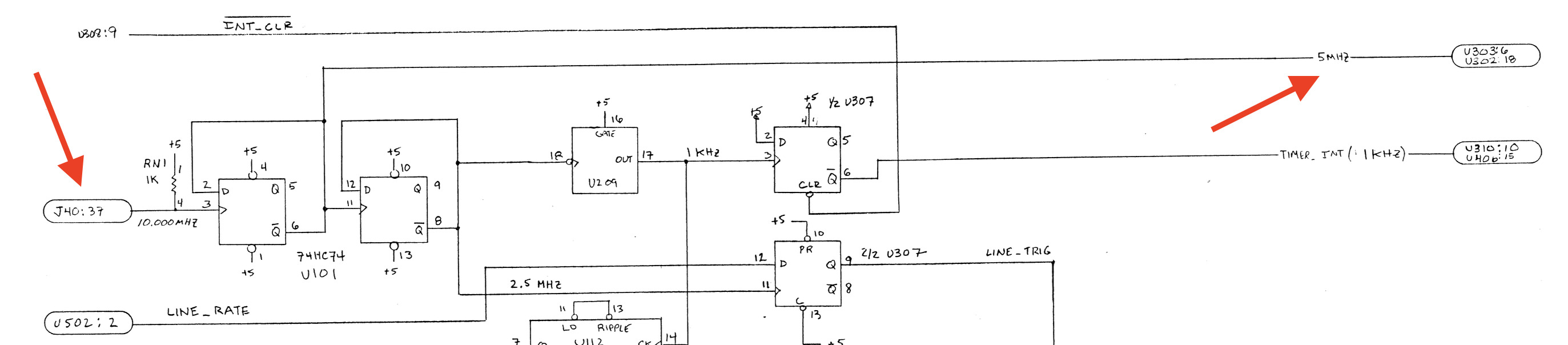 (Click to enlarge)
The 5 MHz CPU clock is derived from the 10 MHz clock, which comes from connector J40: the cable that connects the top and bottom PCB. In other words: if you run the top PCB by itself, there is no clock. And without a clock, the power consumption of the CPU system will be much lower… and with a current boost resistor, the voltage will rise to +7V.
To run the CPU board stand-alone with an active clock, I configured my HP 33120A signal generator to generate a 10 MHz signal and routed its SYNC output to connector J40.
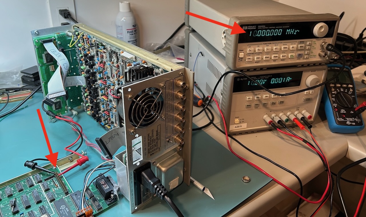 (Click to enlarge)
In the picture above, in addition to the signal generator, you can also see an HP 3631A power supply that outputs 10V: this is a replacement of the reference voltage that’s needed for the dying gasp and reset generator that I mentioned earlier. These are the 2 external signals that are needed to run the CPU top PCB without the analog bottom PCB, though only for a short time: without current boost resistor and cooling fan, the 7805 was now taking on all the current and warming up quickly.
Important: The +12V issue was still there! As soon as the current boost resistor was placed back, it was dissipating 5W and its temperature rose to 130C almost instantly!!!
Side Quest: Debugging the CPU System - Connector Stupidity
With the CPU clock running, I expected some activity on the keyboard/LED and LCD boards, but the CPU seemed stuck.
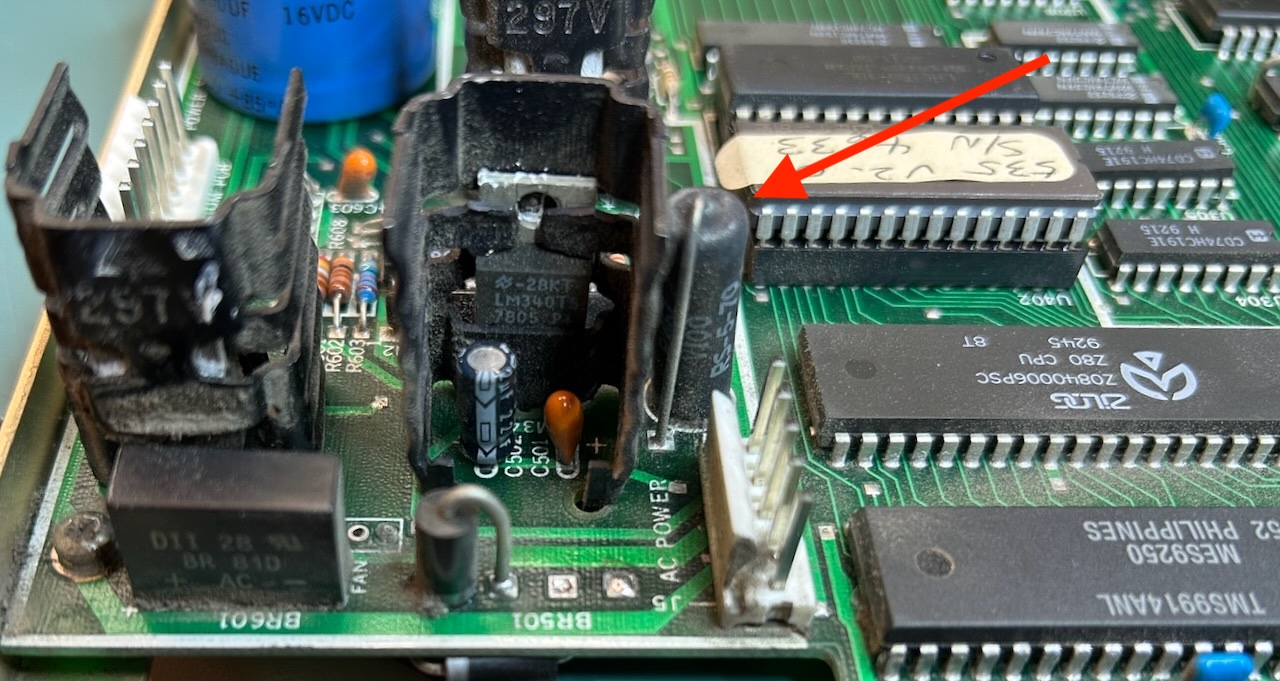
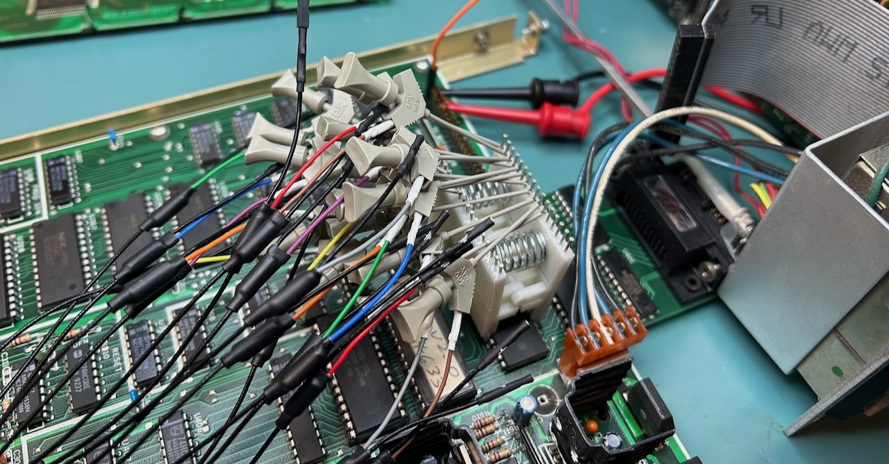
It took a lot of effort to root cause this. I dumped the ROM contents7, used Ghidra to disassemble the code. I also used a logic analyzer to trace the Z80 address bus to get a better insight into what was happening, resulting in this pretty picture:
After many hours, the simple conclusion was this: the connector of the LCD panel cable was plugged in incorrectly. This pulled high a crucial status bit on the data bus which made the Z80 go into an endless loop.
I partially blame SRS for this: the way they deal with connector-related documentation is horrible, unconventional, and inconsistent. Just look at this beauty:
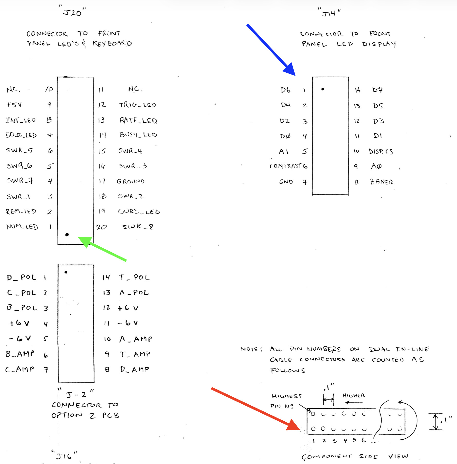
At the bottom right (red), they lay out a pinout convention. The keyboard/LED PCB (green) doesn’t follow that convention. The LCD panel display does follow it, but this is a standard 14-pin interface that’s used by an HD44780-based LCD controller which uses an entirely different convention. They also don’t consistently mark pin 1 on the PCB.
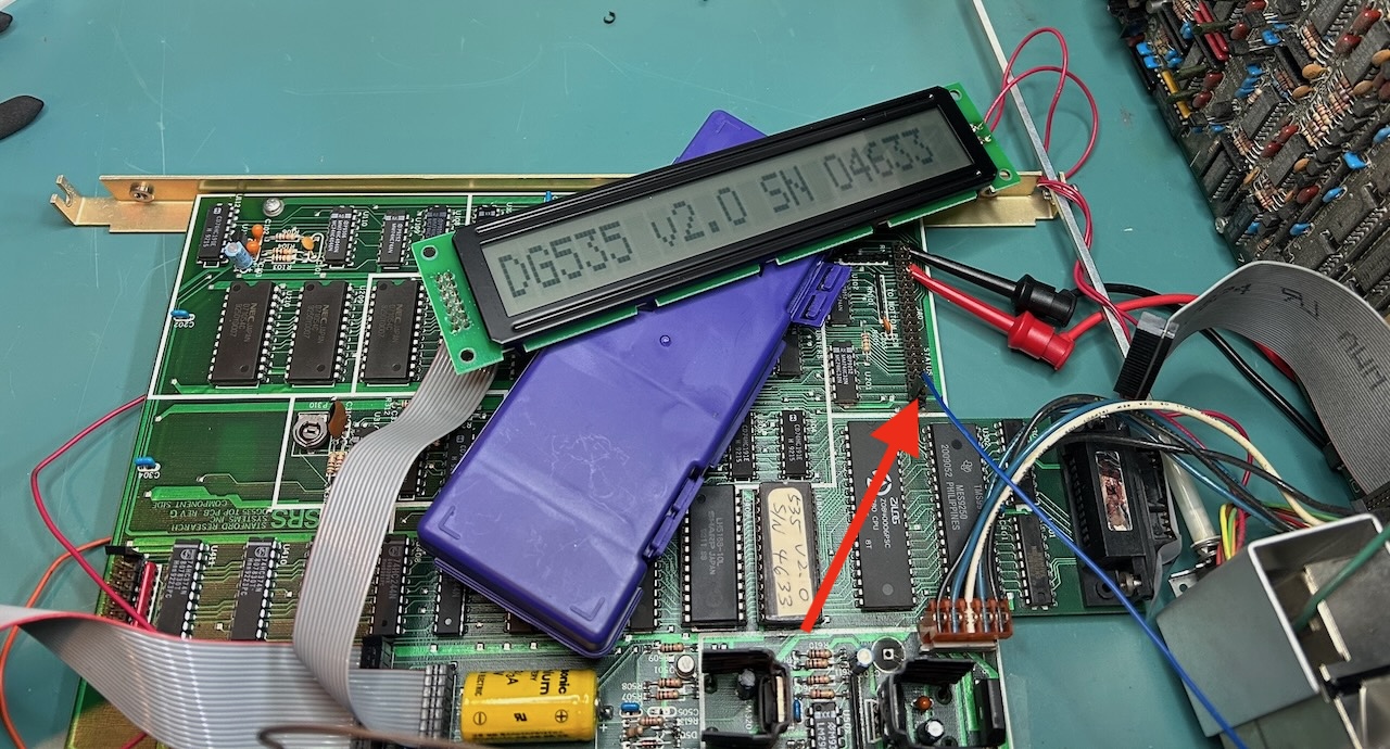
Still, even after fixing that, the LCD didn’t come up. This turned out to be due to another signal that came from the bottom PCB, the analog voltage that sets the LCD contrast. It was sufficient to connect that to ground. That’s the blue wire that the red arrow is pointing to:
The LCD was working now, but without backlight. The backlight of the original LCD panel requires 120V AC with a 50 kOhm resistor in series. This voltage is coming straight from a primary winding of the transformer. I measured 120V just fine, so the backlight was broken. It doesn’t make the display entirely unreadable, but it’s definitely annoying.
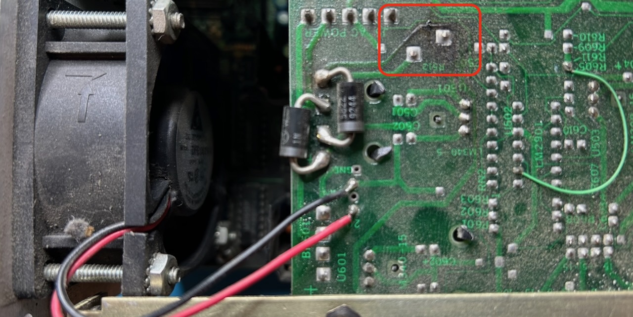
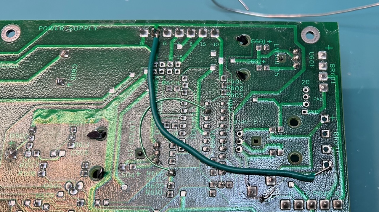
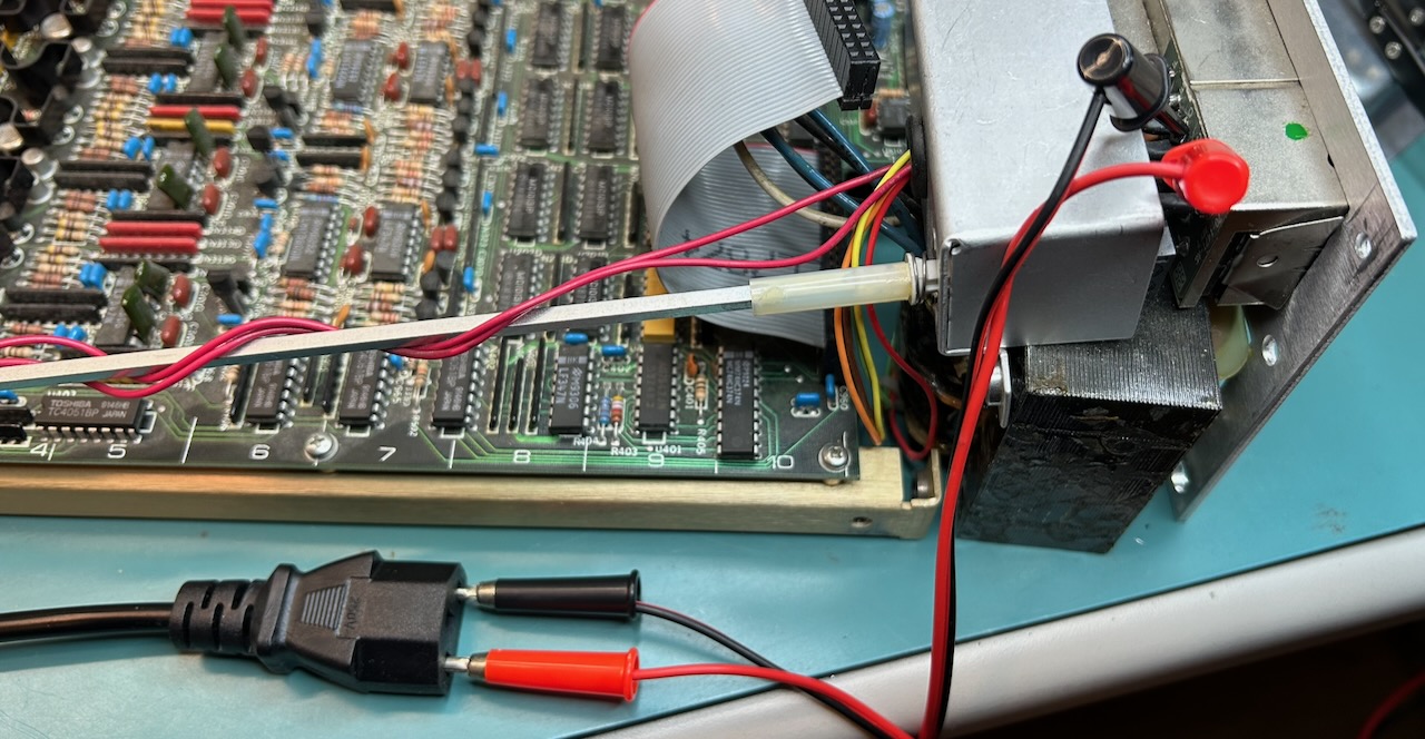
Fixing the Burnt PCB Trace
When I measured the voltages at the start of this journey, I noticed that the -9V was missing on the power connector towards the analog PCB. The trace to this connector is running below the overheating current boost resistor. All I needed to do was install a replacement wire.
Endless Boot Loop after Reassembly
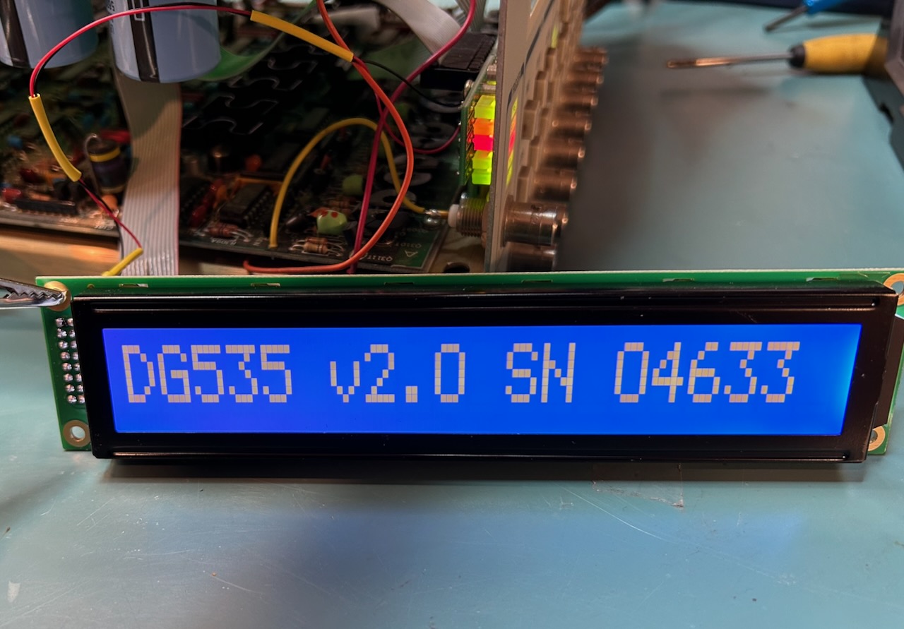
After going through the pain of reassembling the whole unit, I has hopeful that I’d be able to at least operate the keyboard and see things happening on the LCD. That, of course, didn’t happen. Instead, the unit got into an endless boot loop, showing the splash screen, then going blank, repeat.
This cost me another couple of hours to root cause. I disconnected all wires to the top PCB to revert back to the condition where things worked before, but no luck. Eventually, I stumbled onto the “Cold Boot” section in the user manual:
If the instrument turns on, but is completely unresponsive to the keyboard, then the RAM contents may have been corrupted causing the instrument to “hang”. To remedy this situation, turn the unit off, then hold down the BSP (backspace) key down and turn the unit back on again.
Like many old pieces of test equipment, the DG535 uses a BR-2/3A 3V lithium battery to retain settings and calibration values while the unit is powered down. The battery was still good when I measured its voltage, but maybe there was a short circuit due reassembly that made the SRAM loose its contents.
Either way, after following the power-up procedure from the manual the unit worked again.
Note that it’s not necessary to go through a full recalibration after losing the SRAM contents: the EPROM that holds the firmware also contains calibration constants and the serial number that are unique to each unit. That’s pretty cool! The calibration constants are guarded by a checksum to ensure their correctness. What’s puzzling is that the firmware checks the correctness, but when it detects an error, instead of reporting a meaningful error, it does a system reset and retries again, leaving the operator to guess what went wrong.
DG535 Up and Running with a Variac
I still hadn’t tracked down the +12V/-12V on the +9V/-9V rails, but with everything else fixed, I wondered if I could get the full unit to work. Just a few flea markets ago, I had picked up a variac for $15. I always wondered why people need such a thing, and wouldn’t you know it, this was the perfect use case: reduce the mains voltage from 120V AC to ~100V AC to bring down the voltage on the secondary windings of the transformer.
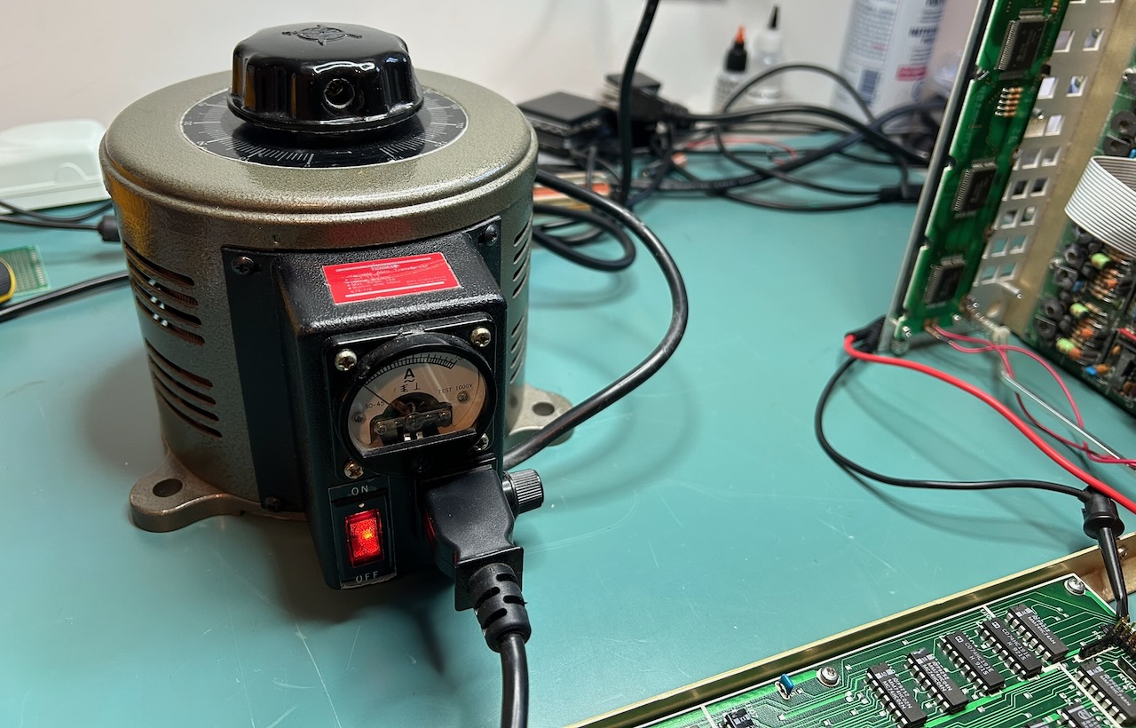
And just like that, the DG535 was working!
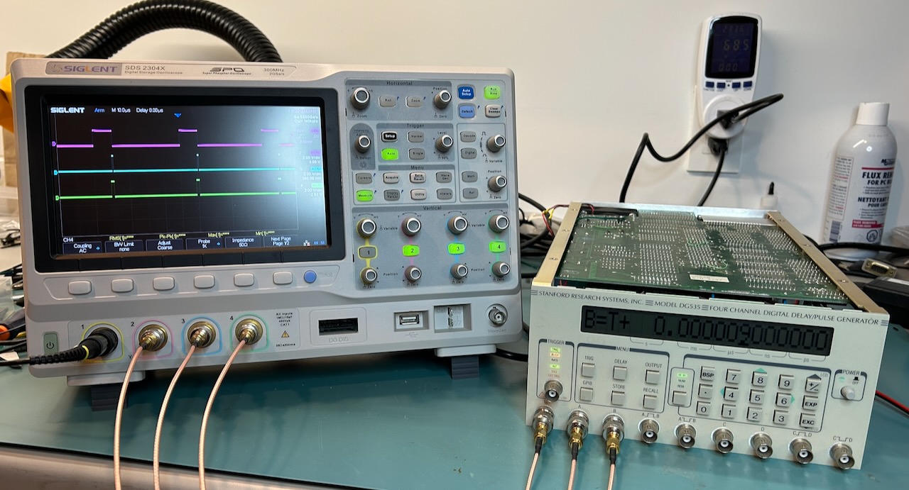
With my SR620 time interval counter and averaging a lot of measurements, I was even able to show that delays could be changed with 5 ps precision.
I measured a power consumption of 62W, not too far away from the 70W that’s specified in the manual, which is just a case of being conservative. Right?
Tracking down the +12/-12V on the +9/-9V Rails
I once again spent a long time trying to track down the 12V vs 9V issue. My only theories were a short somewhere in the transformer, or some wires misconnected during an earlier repair, or the original transformer being replaced by an incorrect one, but extensive and sometimes questionable measurement practises didn’t turn up anything.
Other than secondary winding voltages being too high, the transformer behaved fine.
I started a thread on the EEVblog forum about rewinding a transformer where someone suggested that the output voltage of a transformer can be… load dependent. When only the CPU board was connected, I had measured an overall power consumption of 10W, 60W below specification.
I removed the variac from the setup and measured a power consumption of 72W. The measured voltage on the +9V rail was +10.2V. Enough to raise the power consumption in the 5V current boost resistor from 1.6W to 2.7W, but well within spec of its 5W rating.
The +12V issue was another manifestation of the lack of load resulting in a self-distructing unit! And I had been chasing another ghost.
LCD Replacement
With the unit now fully working, all that remained was fixing the LCD backlight. SRS sells a replacement LCD panel for a ridiculous $200. This must be old stock because you can’t find ones anymore with a 120VAC backlight power supply.
Instead, I bought a CFAH2001B-TMI-ET panel from crystalfontz.com.
It has a 16 pin instead of 14 pin interface, but the 2 additional pins are for the backlight. The original LCD has separate pins for that.
The backlight has an LED with threshold voltage of 3.5v. The typical current is 48mA. The LED connector has a 5V pin already, but the top PCB creates this voltage rail with a 5.1V zener diode and a series resistor from the +15V rail.8 This rail can’t supply 48mA. Instead, I used the +5V pin of the keyboard/LCD PCB nearby, with a 30 Ohm resistor in series, good for a current of (5-3.5)/30 = 50 mA.
The new LCD panel is considerably thicker than the old one, so you can’t reuse the old screws.
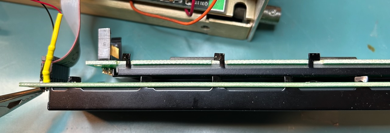
I used Everbilt #4-40 3/8” machine screws from Home Depot instead. Be carefull when tightening those new screws: it’s now possible to overdo things and bend the LCD PCB.
My unit had only 2 out of 4 transformer mounting screws in place. Home Depot didn’t have the #10-32 1 5/8” screws, but slightly shorter #10-32 1 1/2” screws worked fine.
After one more round of carefully connecting all connectors back in place, the DG535 was finally back to where it needed to be:
Post Mortem
A bunch of things went wrong during the design and repair of this DG535.
Design weaknesses:
- Current boost resistors make a design prone to self-destruction due to overvoltage when the system load is too low due to some internal failure.
- Current boost resistors also result in burning out a PCB when the voltage difference between input and output of a voltage regulator becomes too high. This can again happen when the system load is lower than designed for.
- The schematic in the manual shows a discrete diode full bridge for the unregulated +/-9V rail, instead of an integrated one, and no current boost resistor.
- The mechanical design and short cables make it tempting to power the top PCB without connecting the bottom PCB… which cuts down the system load dramatically.
- The power consumption of the top PCB is very low when the bottom PCB is disconnected, due to the lack of 10 MHz clock.
- the pinout of the connectors of the DG535 doesn’t follow standard convention, and the convention that is documented in the manual is violated on the same page.
- The schematic of the top PCB shows a +/-9V rail. The bottom PCB schematic shows +/-8V rails on the same connector pins. In reality, the measured voltage is 10.2V. Confusing.
Repair mistakes:
- A previous attempt at repairing saw the replacement of an integrated diode bridge by a discrete one. To make things worse, they used 1N5822 Schottky diodes, as shown in the incorrect schematic. Schottky diodes have a threshold voltage of 0.4V instead of a 0.7V threshold for the integrated diode bridge. Because of this, the unregulated DC output was 2 x (0.7 - 0.4V) = 0.6V higher, which increased the power consumption in the current boost resistors even more!
- PCBs were powered on without full load. This resulted in PCB traces burning up.
- Connectors were incorrectly plugged in. I should have taken pictures before disconnecting anything.
- I knew not enough about transformers and wasted way too much time chasing a ghost because of it!
In the end, I only made 3 real fixes:
- removed the discrete diode bridge and replaced it by an integrated one
- installed a bodge wire to bring the -9V to the top-to-bottom PCB power connector
- replaced the LCD panel with broken backlight by a new one with diode backlight
I got lucky that the 5V digital components survived being exposed to 7V. One thing that I’ve learned over the years is that old ICs are pretty good at surviving that kind of abuse.
References
- Stanford Research - DG535 Digital Delay Generator
- Analog Devices - Single Resistor Provides Extra Current from a Linear Regulator
- EEVblog forum - SRS Stanford Research DG535
- EEVblog forum - Rewinding a power transformer?
Footnotes
-
Not that I’ve ever done that, but it’s what I tell my wife. ↩
-
Whether or not it will ever sell for that asking price is a different story. ↩
-
NIM stands for Nuclear Instrumentation Model. It’s a voltage and current standard for fast digital pulses for physics and nuclear experiments. ↩
-
When dealing with mirror image of an IC footprint, I’m constantly second guessing myself about whether or not I’m probing the right pin. ↩
-
When the +9V voltage rail drops below +7.5V, the dying gasp circuit creates a non-maskable interrupt to the CPU, allowing to quickly store data in non-volatile RAM before the power is completely gone. ↩
-
I emailed SRS to ask if they had an updated schematic, but they told me to send in the unit for repair. ↩
-
The ROM contents of each DG535 are unique for that particular unit, since they contain the serial number and calibration data that were determined in the factory. If you program the EPROM with my ROM file in your unit, expect delay specification to be significantly worse. ↩
-
I have no idea why SRS didn’t use the regular +5V rail to power the LCD panel. ↩