Rohde & Schwarz AMIQ Modulation Generator - Teardown and Analog Deep Dive
- Introduction
- The Rohde & Schwarz AMIQ Modulation Generator
- WinIQSim Software
- Inside the AMIQ
- The Signal Generation PCB
- Analog Signal Generation Architecture: Fixed vs Variable DAC Clock
- Internal Reference Clock Generation
- DAC Clock Synthesizer
- I/Q Output Skew Tuning
- Variable Gain Amplifier
- Internal Diagnostics
- Efficient Distribution of Configuration Signals
- Conclusion
- References
Introduction
Every few months, a local company auctions off all kinds of lab, production and test equipment. I shouldn’t be subscribed to their email list but I am, and that’s one way I end up with more stuff that I don’t really need.
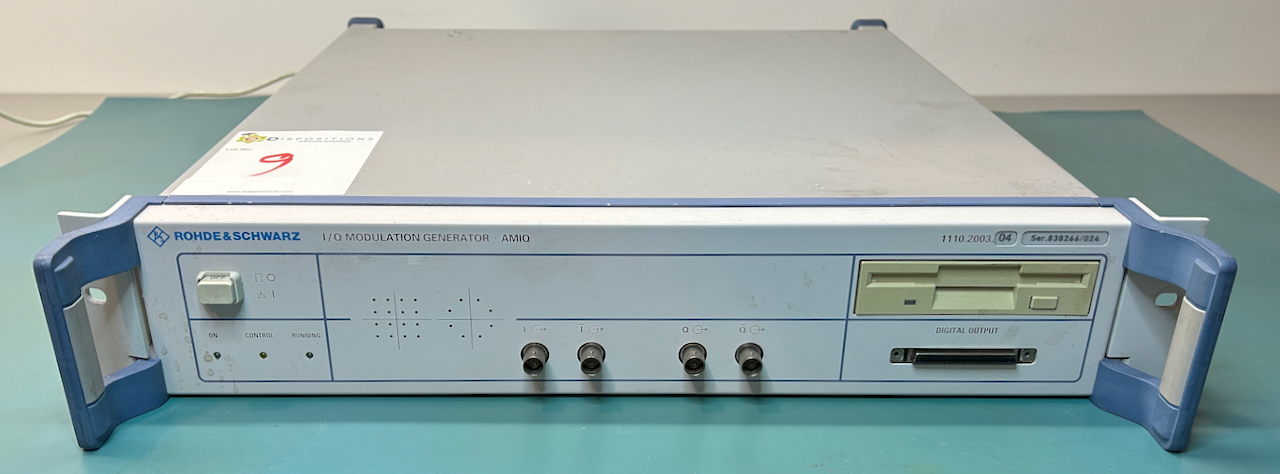
During a recent auction, I got my hands on a Rohde & Schwarz AMIQ, an I/Q modulation generator, for a grand total of $45. Add to that another 30% for the auction fee and taxes and you’re still paying much less than what others would pay for a round of golf? But instead of one morning of fun, this thing has the potential to keep me busy for many weekends, so what a deal!
 (Click to enlarge)
A few days after “winning” the auction, I drove to a dark dungeon of a warehouse in San Jose to pick up the loot.
The AMIQ has a power on/off button and 3 LEDs and that’s in terms of user interface. There are no dials, there’s no display. So without any other options, I simply powered it up and I was immediately greeted by the ominous clicking of a hard drive. I was right: this thing would keep me entertained for at least a little bit!
 (Click to enlarge)
It took a significant amount of effort to restore the machine back to its working state. I’ll write about that in future blog posts, but let’s start with an overview of the functionality and a teardown of the R&S AMIQ and then deep dive into some of its analog circuits.
AMIQ prices on eBay vary wildly, from $129 to $2600 at the time of writing this. Even if you get one of the higher priced ones, you should expect to get a unit that’s close to failing due to leaking capacitors and a flaky harddrive!
The Rohde & Schwarz AMIQ Modulation Generator
Reduced to an elevator sales pitch, the AMIQ is a 2-channel arbitrary waveform generator (AWG) with a deep sample buffer. That’s it!
It has a streaming buffer that feeds samples to 2 14-bit DACs at a sample rate of up to 105MHz. Two output channels I and Q will typically contain quadrature modulation signals that are sent to an RF vector signal generator such as a Rohde & Schwarz SMIQ for the actual high-frequency modulation. In a typical setup, the AMIQ is used to generate the baseband modulated signal and the SMIQ shifts the baseband signal to an RF frequency.
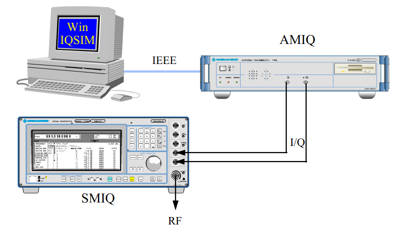
Since the AMIQ has no user interface, the waveform data must provided by an external device. This could be a PC that runs R&S WinIQSim software or even the SMIQ itself because it has the ability to control an AMIQ. You can also create your own waveforms and upload them via floppy disk, GPIB or an RS-232 interface using SCPI control commands.
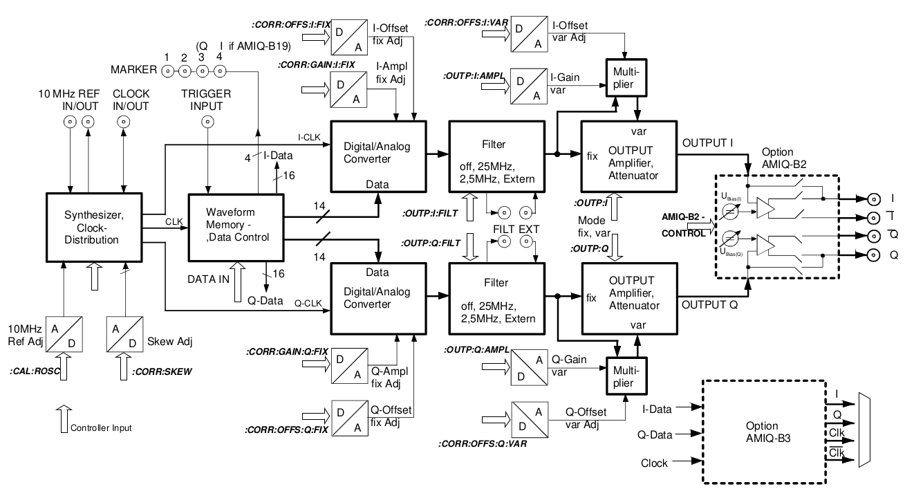
Figure 4-1 of the AMIQ Operating Manual has a simplified block diagram. It is pretty straightforward and somewhat similar to the one of my HP 33120A function generator:
 (Click to enlarge)
On the left are 2 blocks that are shared:
- a clock synthesizer
- waveform memory
And then for each channel:
- 14-bit D/A converter
- analog filters
- output section with amplifier/attenuator
- differential analog output driver (AMIQ-B2 option)
The major blocks are surrounded by a large amount of DACs that are used to control everything from the tuning input of local 10MHz clock oscillator, gain and offset of output signals, clock skew between I and Q signal and much more.
You could do some of this with a modern SDR setup, but the specifications of the AMIQ units are dialed up a notch. Both channels are completely symmetrical to avoid modulation errors at the source. If there’s a need to compensate for small delay differences in, for example, the external cables, you can compensate for that by changing the skew between clocks of the output DACs with a precision of 10ps. Similarly, the DAC sample frequency can be programmed with 32-bit precision.
 (Click to enlarge)
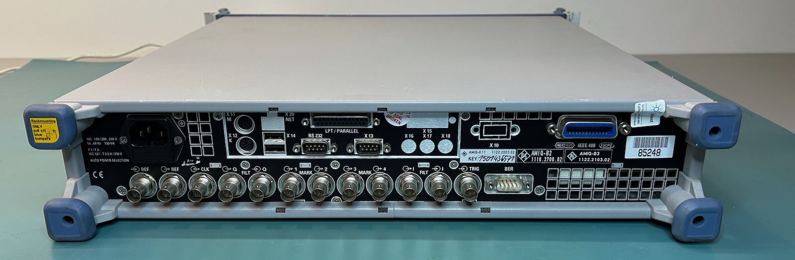
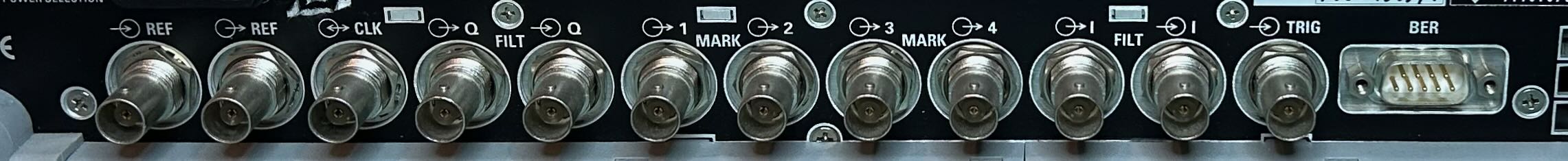
In addition to the main I/Q outputs at the front, there are a bunch of secondary input and output signals:
- 10MHz reference input and output
- sample clock
- trigger input
- marker output
- external filter loopback output and input
- bit error rate measurement (BER) connector (AMIQ-B1 option)
- parallel interface with the digital value of the samples that are sent to the DAC (front panel, AMIQ-B3 option)
 (Click to enlarge)
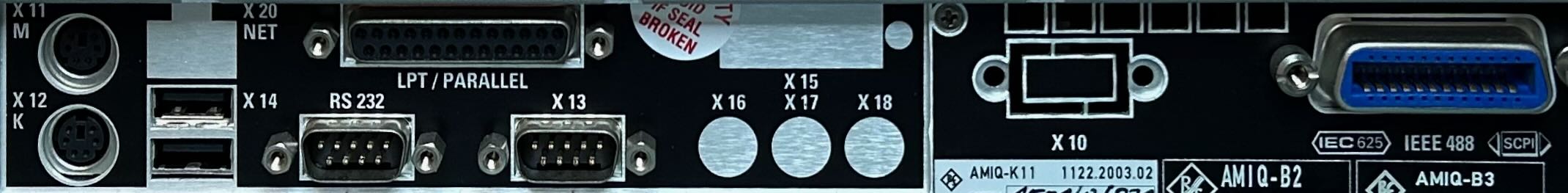
Above those speciality inputs and outputs are the obligatory GPIB interface and a bunch of generic connectors that look suspiciously like the ones you’d find on an early century PC:
- PS/2 keyboard and mouse
- Parallel port
- RS232
- USB
There are 3 different AMIQ versions:
- 1110.2003.02: 4M samples
- 1110.2003.03: 4M samples
- 1110.2003.04: 16M samples
Mine is an AMIQ-04.
WinIQSim Software
While it is possible to control the AMIQ over RS-232 or GPIB with your own software, you’d have a hard time matching the features of WinIQSim, a R&S Windows application that supports the AMIQ.
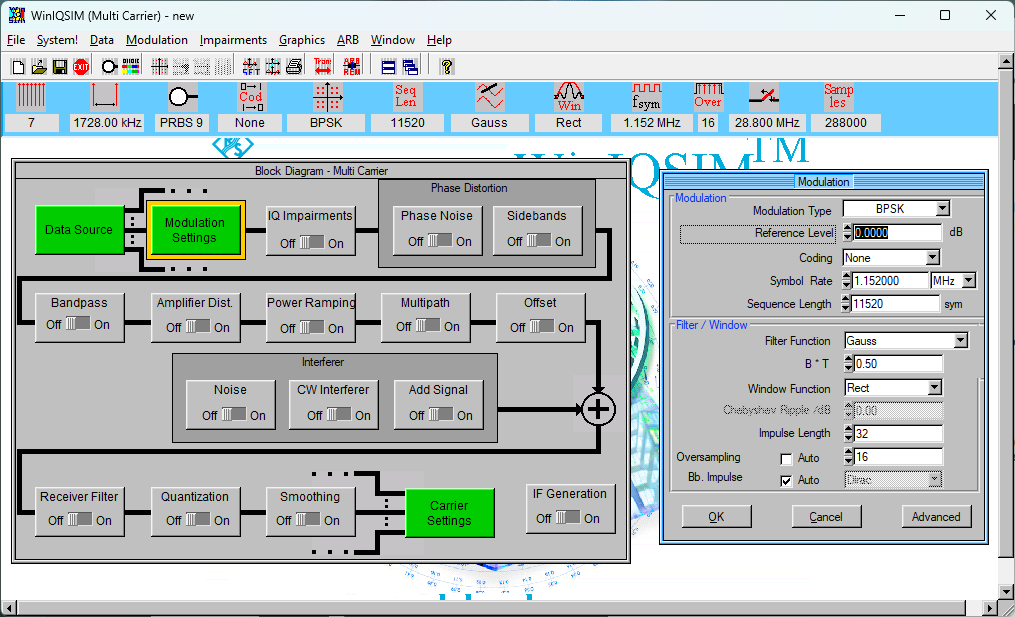 (Click to enlarge)
With WinIQSim, you can select one of the popular communication protocols from the late nineties and early 2000s, fill in digital framing data, apply all kinds of distortions and interferences, compute the I and Q waveforms and send it to the AMIQ.
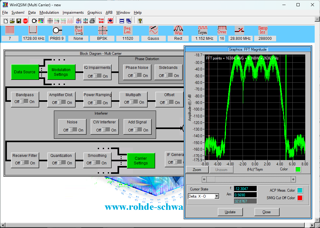
Some of the supported formats include CDMA2000, 802.11a WLAN, TD-SCDMA and more. But you don’t have to use these official protocols, WinIQSim supports any kind of FSK, QPSK, QAM or other common modulation method.
You need a license for some of the communication protocols. The license is linked to the AMIQ device, not the PC, but the license check is pretty naive, and while I haven’t tried it… yet, the EEVblog forum has discussions about how to enable features yourself. My device only came with a license for IS-95 CDMA.
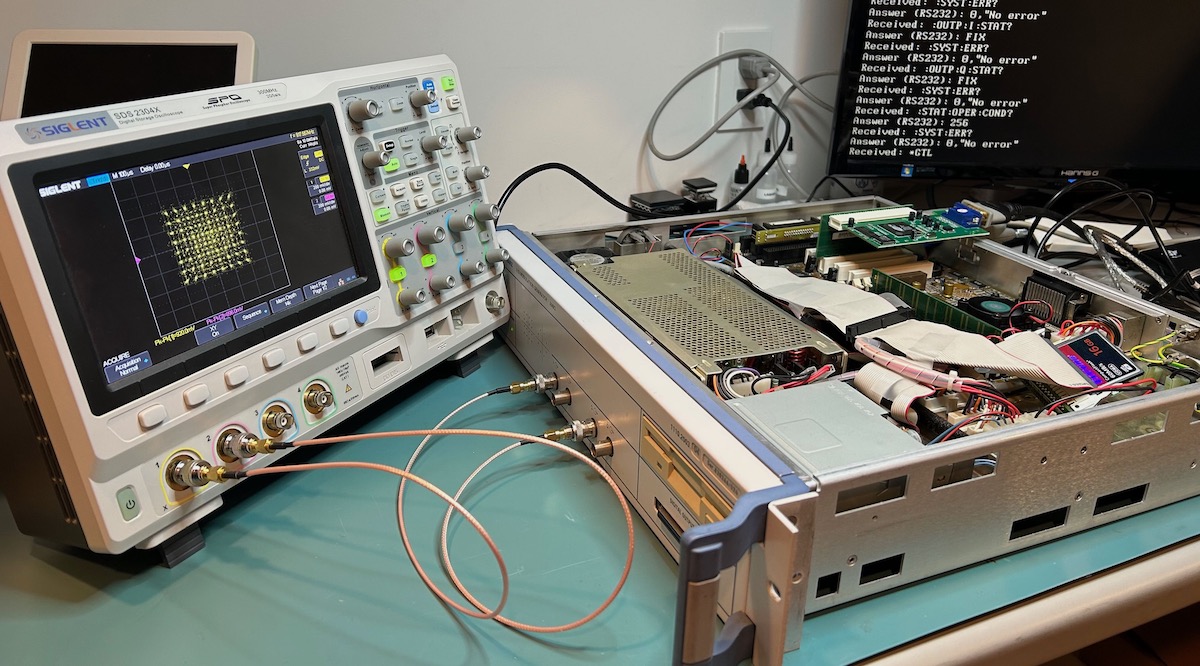
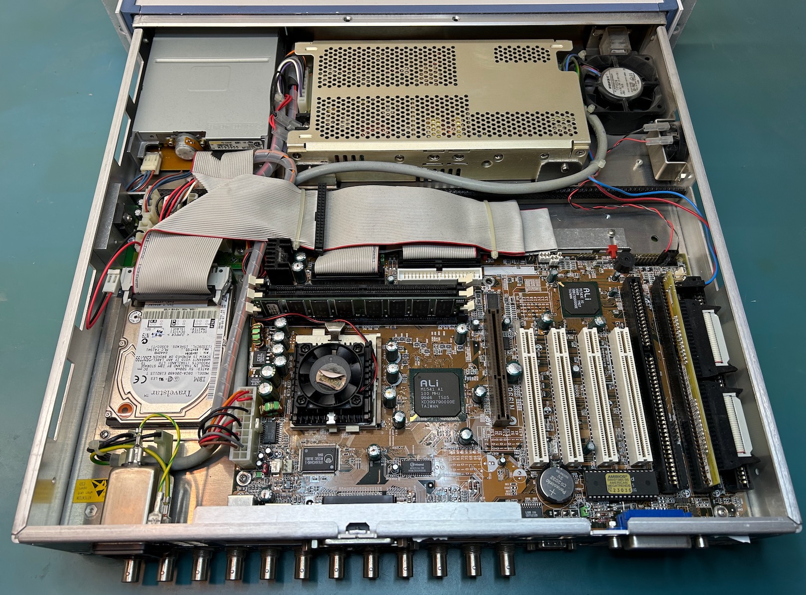
Inside the AMIQ
It’s trivial to open up an AMIQ: after removing the 4 feet in the back with a regular Philips screwdriver, you can simply slide off the outer case.
It has 2 major subsystems:
-
the top contains all the components of a standard PC
 (Click to enlarge)
 -
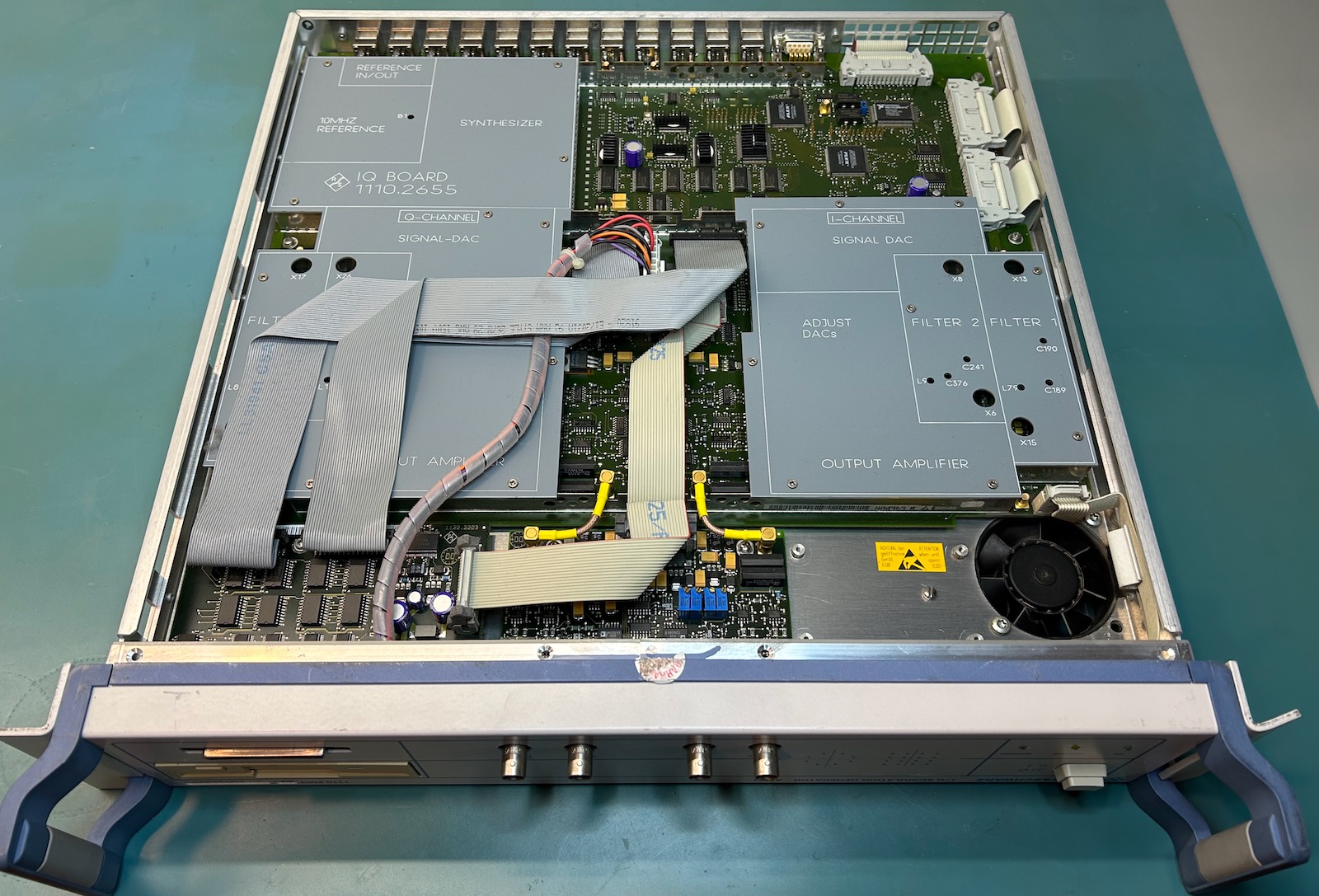
the bottom has a signal generation PCB
 (Click to enlarge)
The PCB looks incredibly clean and well laid out and I love how they printed the names of different sections on the metal gray shielding plates.
We’ll leave the PC system for a future blog post, and focus on the signal generation PCB.
The Signal Generation PCB
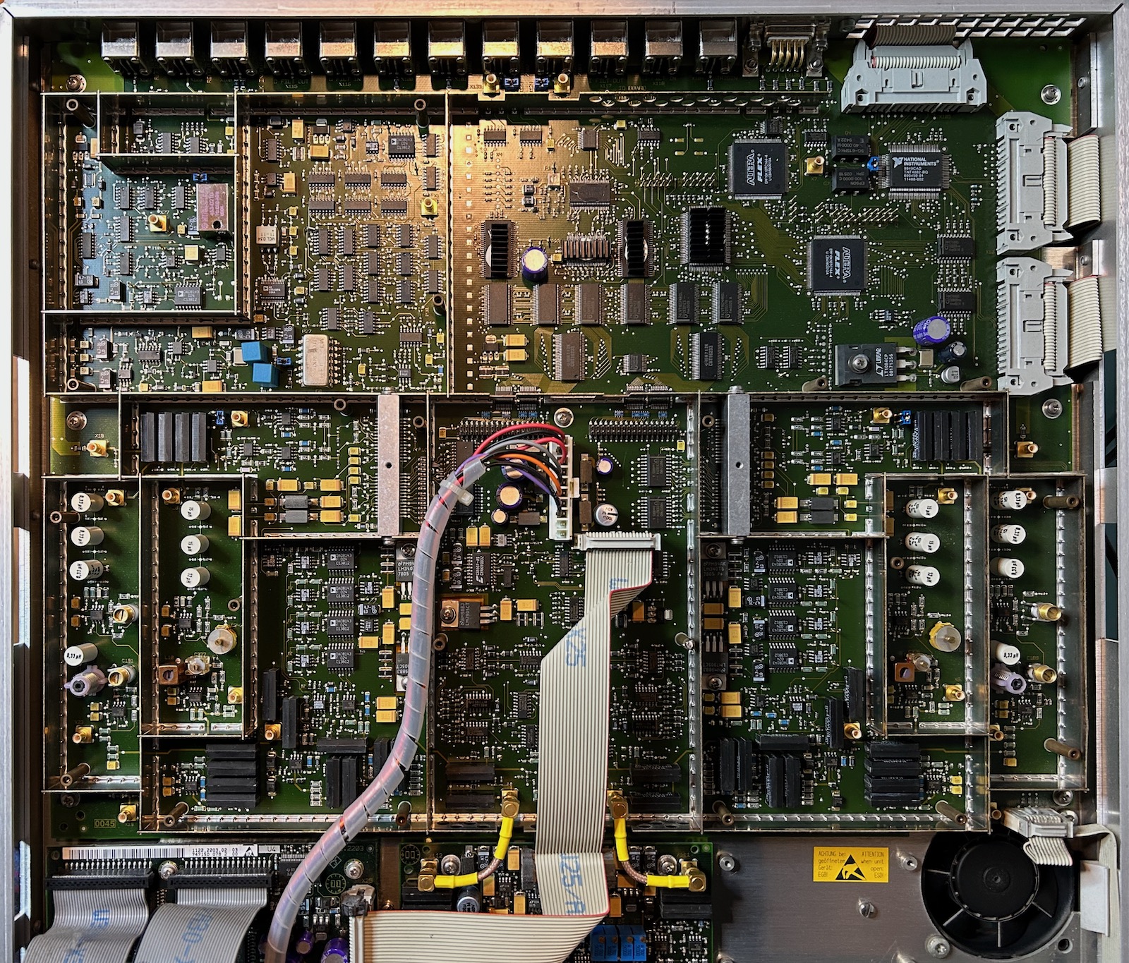
Let’s remove the shielding plates to see what’s underneath. I had to drill out one of the screws that attach the plates because the head was stripped. (Did somebody before me already try to repair it?)
 (Click to enlarge)
The bottom half left and right sections are perfectly symmetrical, as one would expect for a device that has the ability to tune skew mismatches with a 10 ps precision.
Annotated, it looks like this:
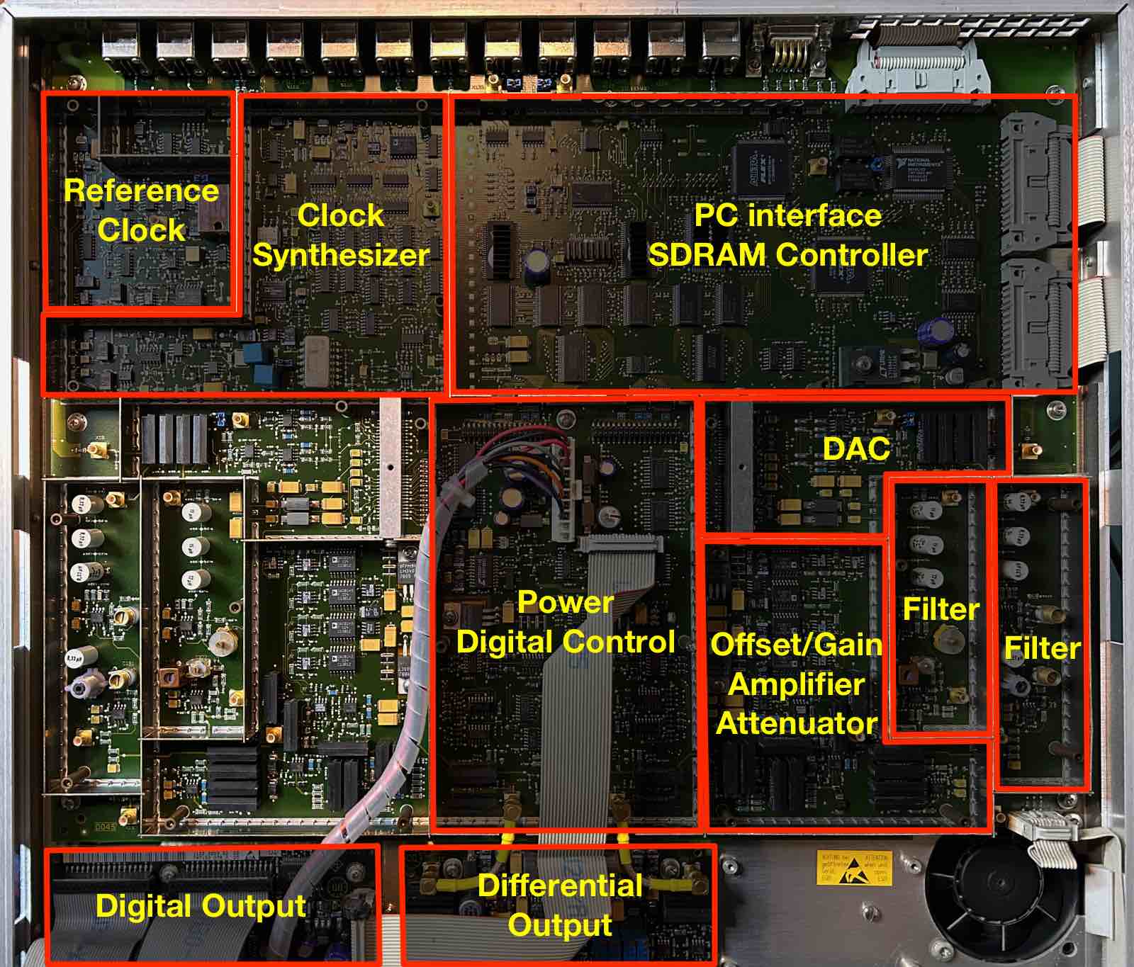 (Click to enlarge)
Rohde & Schwarz recently made the terrible decision to lock all their software and manuals behind an approval-only corporate log-in wall, but luckily some of the most important AMIQ assets can be found online elsewhere, including the operating manual and a service manual that contains the full schematics!
Let’s dig a bit deeper into the various aspects of the design.
In what follows I’ll be focusing primarily on analog aspects of the design. This is a very personal choice: not that the digital sections aren’t important, it’s just that, as digital design engineer, they’re not particular interesting to me. By studying the analog sections, I hope to stumble into circuits that I didn’t really know a lot about before.
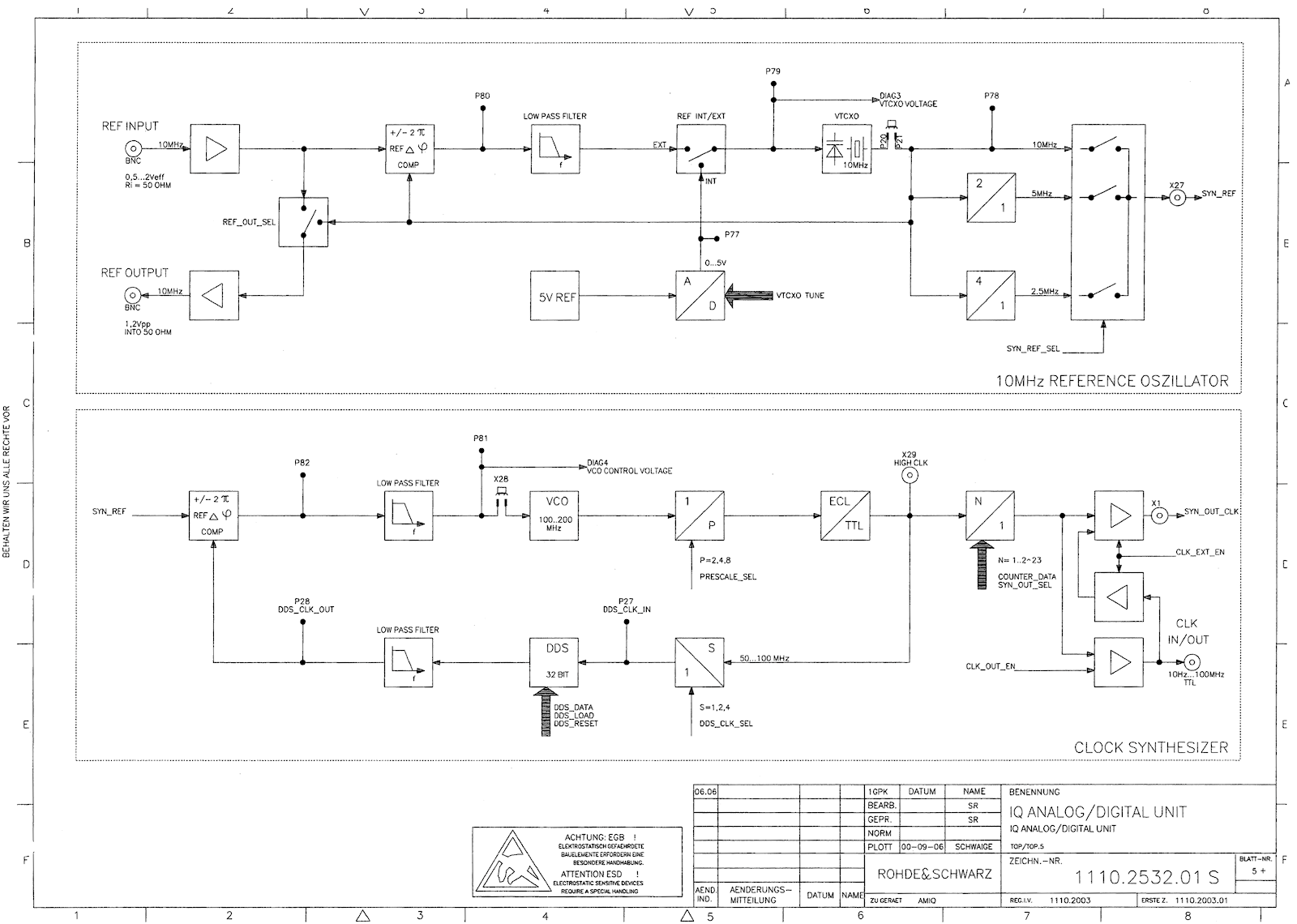
Fantastic Schematics
Before digging in for real, a word about the schematics: they are fantastic.
Each sub-system has a block diagram that is already pretty detailed, with signal names that match the schematics and test points, often with annotations to indicate the voltage or frequency range. Here’s the block diagram of the reference and DAC clock generation section, for example.
Signals that come from or go to other pages are fully referenced. Look at the SYN_OUT_CLK signal below:
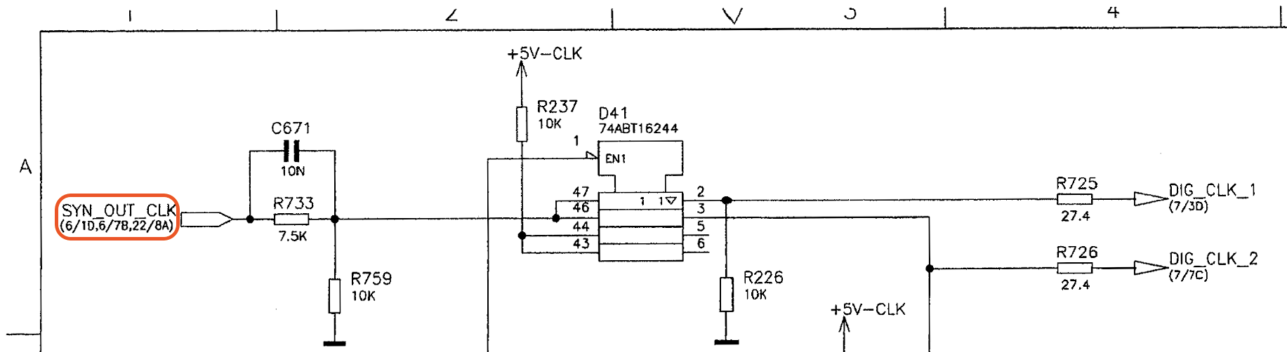
The signal is also used on page 6, coordinate 1D and 7B and page 22, coordinate 8A. How cool is that?
Signal path test points
One of the awesome features of the PCB is the generous amount of test points. We’re not just talking PCB test point against which you can hold your oscilloscope probe or even header pins, though there are plenty of those too, but full on SMB connectors.
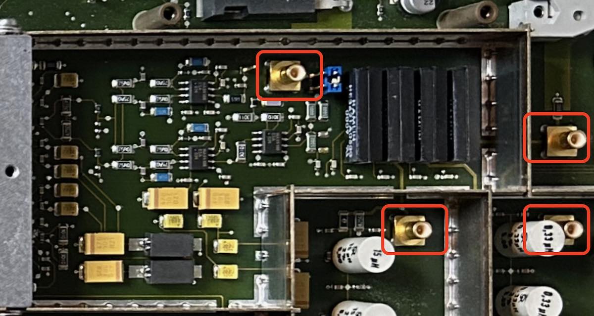
In addition to these SMD connectors, there are also plenty of jumpers that can be used to interrupt the default signal flow and insert your own test signal instead.
Analog Signal Generation Architecture: Fixed vs Variable DAC Clock
In the HP 33120A the DAC has a fixed 40 MHz clock. There’s a 16 kB waveform RAM that contains, say, one quarter period of a 100 Hz sine. If you want to send out a sine wave of 200 Hz, instead of sequentially stepping through all the addresses of the waveform RAM, you just skip every other address. One of the benefits of this kind of generation scheme is that you can make do with a fixed frequency analog anti-aliasing filter: the Nyquist frequency is always the same after all.
A major disadvantage, however, is that even if the output signal has a bandwidth of only 1MHz, you still need to feed the DAC at the fixed clock rate. You could insert a digital upsampling filter between the waveform memory and the DAC, but that requires significant mathematical DSP fire power, or you’d have to increase the depth of the waveform memory.
For an arbitrary waveform generator, it makes more sense to run the DAC at whichever clock speed is sufficient to meet the Nyquist requirement of the desired signal and provide a number of different filtering options. The AMIQ has 4 such options: no filter, a 25 MHz, a 2.5 MHz or a loopback through an external filter.
The DAC sample clock range is huge, from 10 Hz all the way to 105 MHz, though specifications are only guaranteed up to 100 MHz. According to the data sheet, the clock frequency can be set with a precision of 10^-7.
Internal Reference Clock Generation
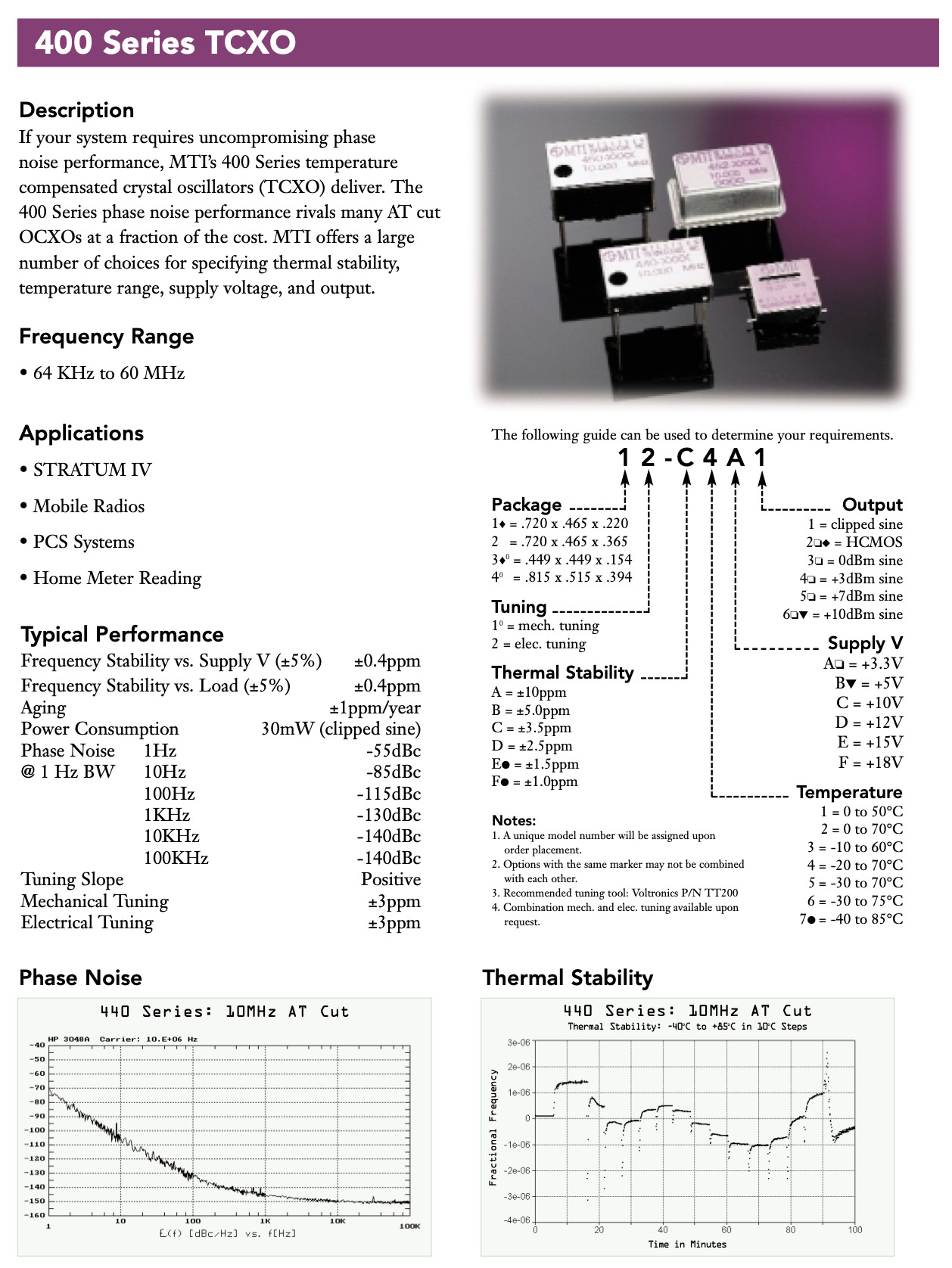
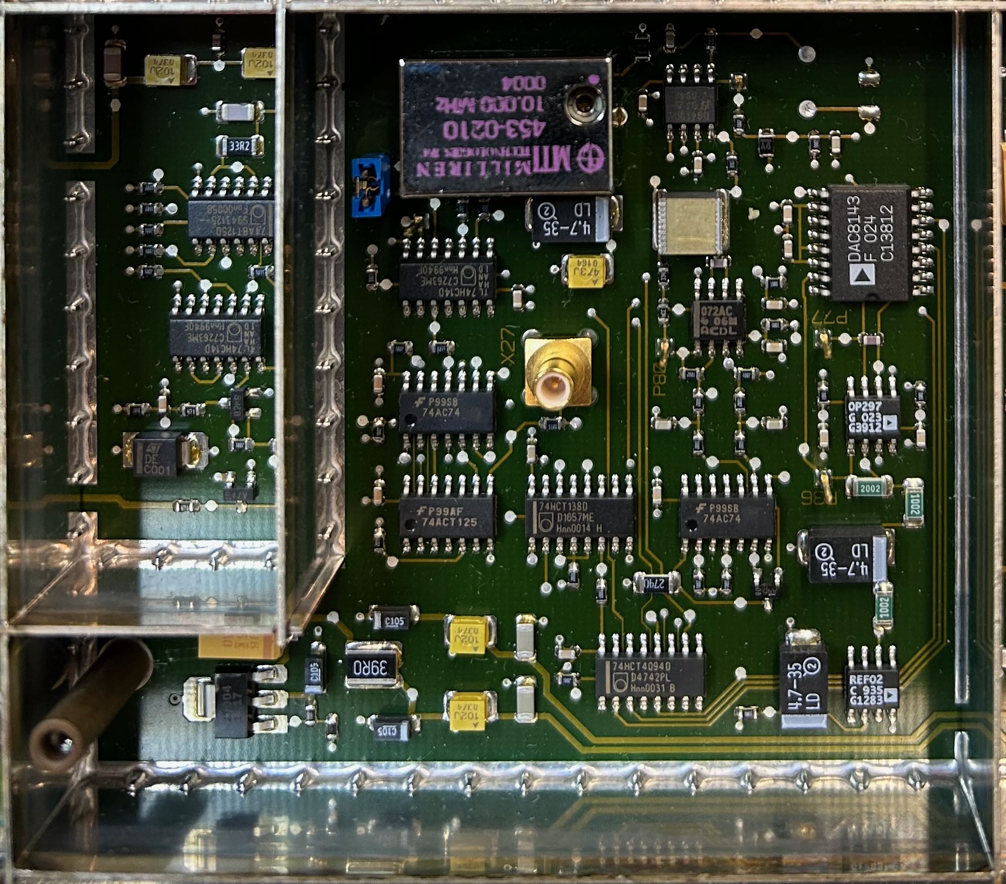
Like all professional test and measurement equipment, the AMIQ uses a 10MHz reference clock that can come from outside or that can be generated locally with a 10MHz crystal. It’s common for high-end equipment to have an oven controlled crystal oscillator (OCXO), but AMIQ has a lower spec’ed temperature controlled one (TCXO), a Milliren Technologies 453-0210.
If we look at the larger reference clock generation block diagram, we can see something slightly unusual: instead of selecting between the internal TCXO output or the external reference clock input, the internal reference clock always comes from the TCXO (green).
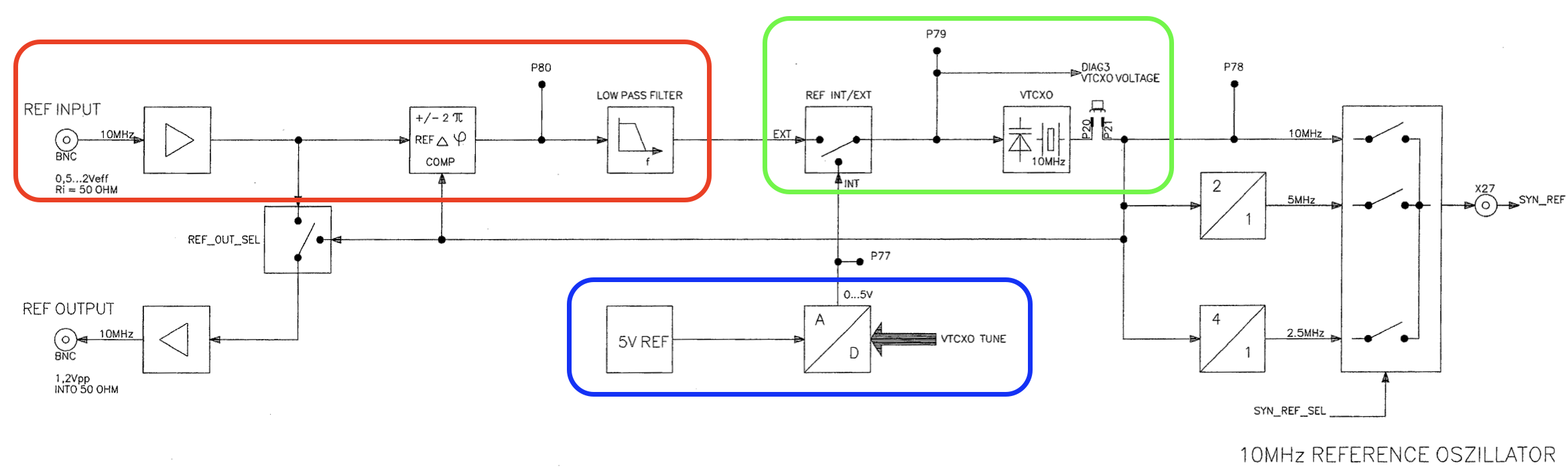
When the internal clock is selected, the TCXO output frequency can be tuned with an analog signal that comes from
the VTXCO TUNE DAC (blue), but when the external reference input is active, the TCXO is phase locked to the
external clock. You can see the phase comparator and low pass filter in red.
The reason for using a PLL with the internal TCXO as the voltage controlled oscillator is probably to ensure that the generated reference clock has the phase noise of the TCXO while tracking the frequency of the external reference clock: a PLL acts as a low-pass filter to the reference clock and as a high-pass filter to the VCO. If the TCXO has a better high frequency phase noise than the external reference clock, that makes sense. This is really out of my wheelhouse, so take all of this with a grain of salt…
SYN_REF is the output of the internal reference clock generation unit.
DAC Clock Synthesizer
The clock synthesizer creates a highly programmable DAC clock from the internal reference clock SYN_REF from
previous section. It should come as no surprise that this clock is generated by a PLL as well.
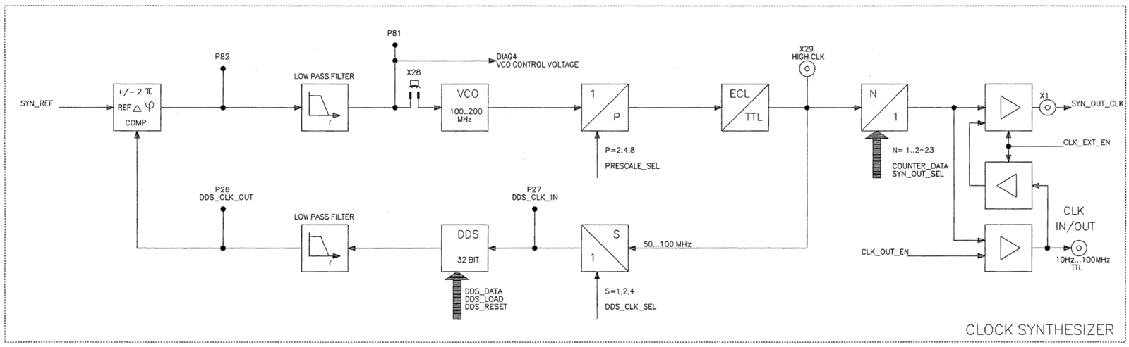
There are two speciality components in the clock generation path:
- a Mini-Circuits JTOS-200 VCO
- an Analog Devices AD9850 DDS Synthesizer
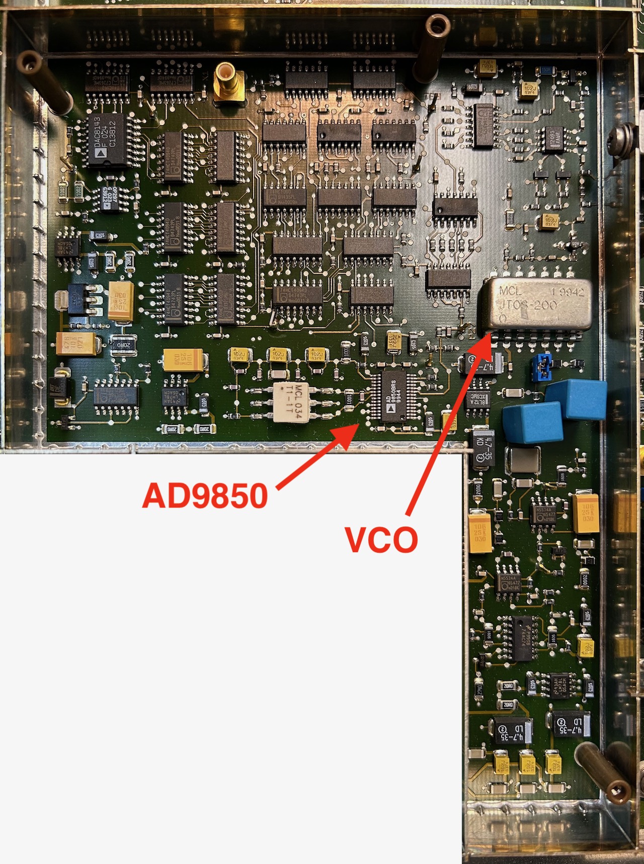 (Click to enlarge)
The VCO has an operating frequency between 100 and 200 MHz. I don’t know enough about VCOs to give meaningful commentary about the specifications, but based on comparisons with similar components on Digikey, such as this FMVC11009, it’s safe to assume that it’s an expensive and high quality component.
The AD9850 is located in the feedback path of the PLL where it acts as a feedback divider with a precision of 32 bits.
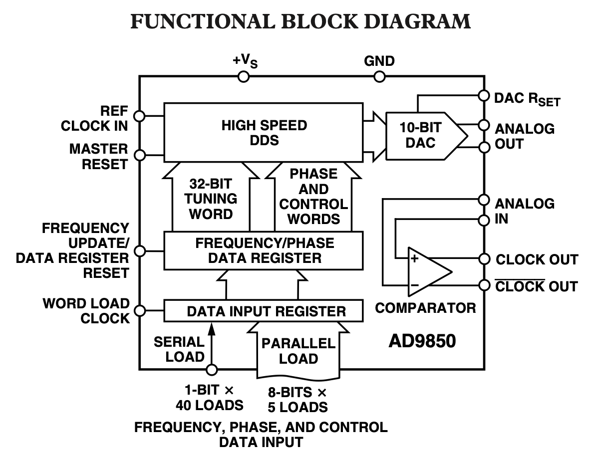
The signal flow inside the AD9850 is interesting:
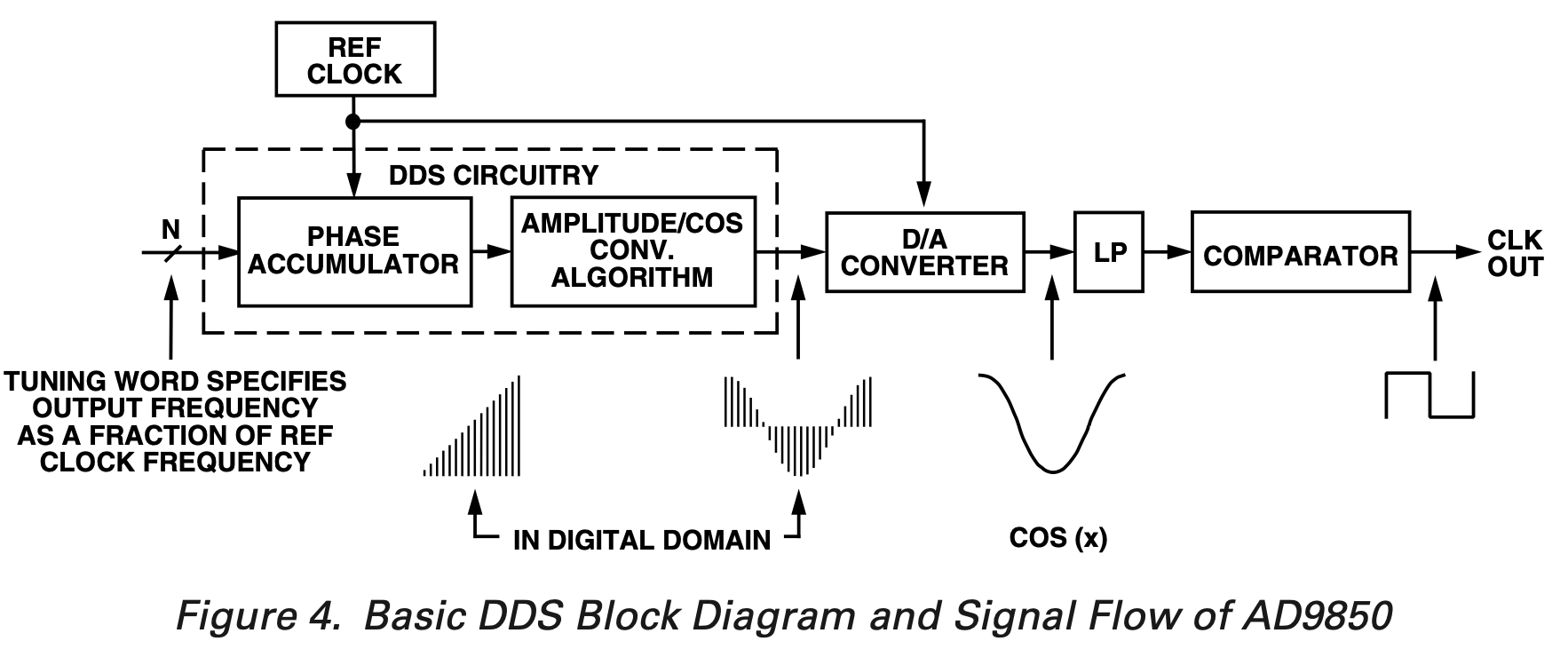
It works as follows:
- each clock cycle, the phase of a numerical controlled oscillator (NCO) accumulates with the programmable 32-bit increment.
- the upper bits of the phase accumulator serve as the address of a sine waveform table.
- a 10-bit DAC converts the digital sine wave to analog.
- the analog signal is sent through an external low-pass filter.
- the output of the low-pass filter goes back into the AD9850 and through a comparator to generate a digital output clock.
This thing has its own programmable signal generator! But why the roundtrip from digital to analog back to digital? In theory, the MSB of the NCO could be used as output clock of the clock generator.
The problem is that in such a configuration, the length of each clock period toggles between N and N+1 clock cycles, with a ratio so that the average clock period ends up with the desired value. But this creates major spurs in the frequency spectrum of the generated clock.
When fed into the phase comparator of a PLL, these frequency spurs can show up as jitter at the output of the PLL and thus into the spectrum of the generated I and Q signals.
By converting the signal to analog and using a low pass filter, the spurs can be filtered away. The combination of a low pass filter and a comparator acts as an interpolator: the edges of the generated clock fall somewhere in between N and N+1.
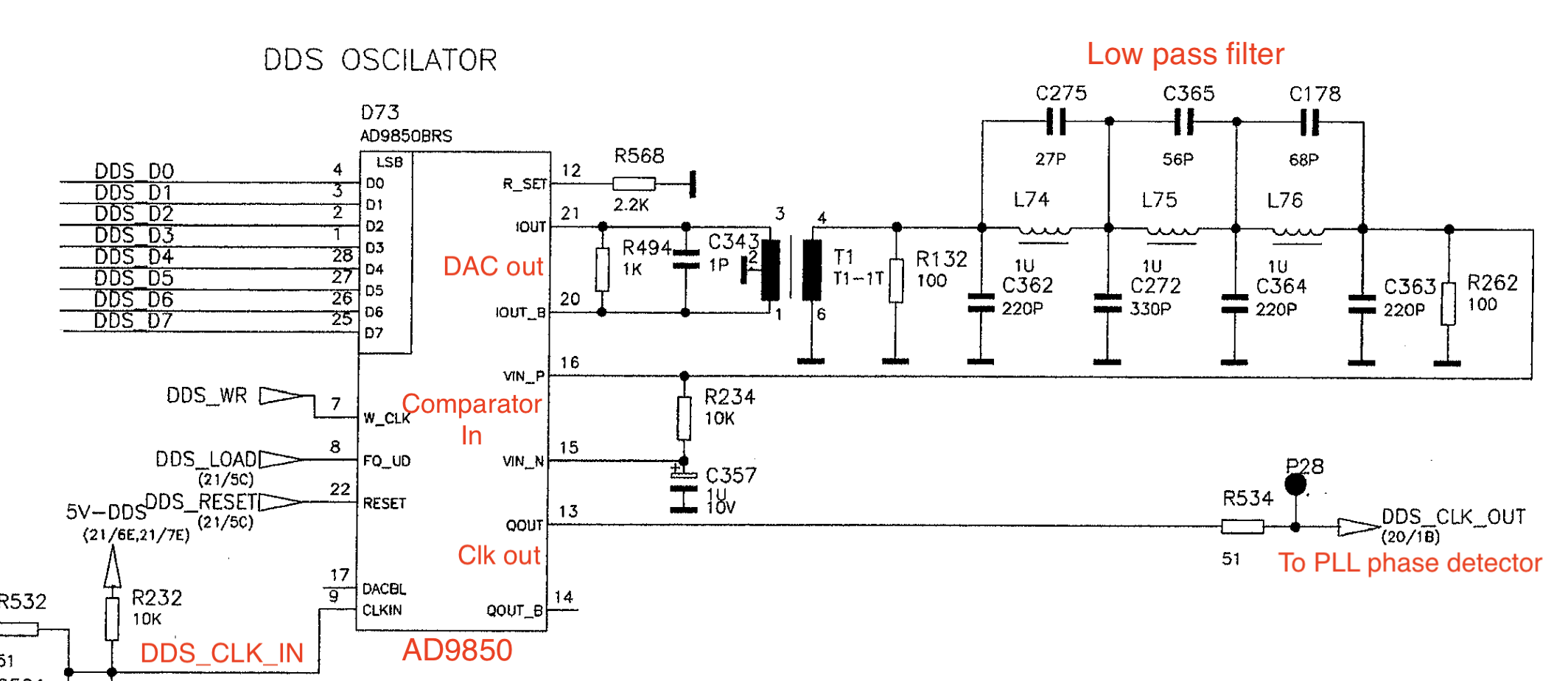
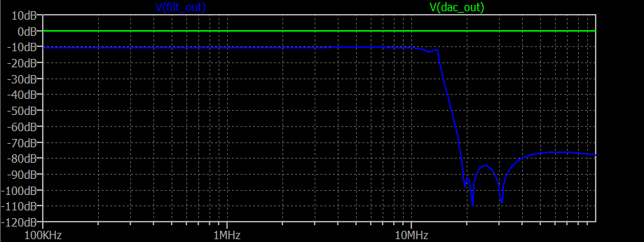
The steepness of the low pass filter depends on the ratio between the input and the output clock: the lower the ratio, the steeper the filter. There are a bunch of binary clock dividers that make it hard to know the exact ratio, but if the output of the VCO is 100 MHz and the input 10 MHz or less, there is a 10:1 ratio. The AMIQ has a 7th order elliptical low pass filter.
I ran a quick simulation in LTspice to check the behavior.
(dds_filter.asc source file.)
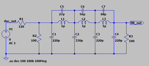
The filter has a cut-off frequency of around 13 MHz:
In modern fractional PLLs, instead of using a regular DAC, one could use a high-order sigma-delta unit to create a pulse density modulated output with the noise pushed to higher frequencies and a low pass filter that can be less aggressive.
There’s a plenty of literature online about DDS clock generators, some of which I’ve listed in the references at the bottom, but the datasheet of the AD9850 itself is a good start.
I/Q Output Skew Tuning
Earlier I mentioned the ability to tune the skew between the I and the Q output to compensate for a difference in cable length when connecting the AMIQ to an RF signal generator.
While the digital waveform fetching circuit works on one clock, the two clocks that go to the DAC are the ones that can be changed:

Here’s what the skewing circuit looks like:
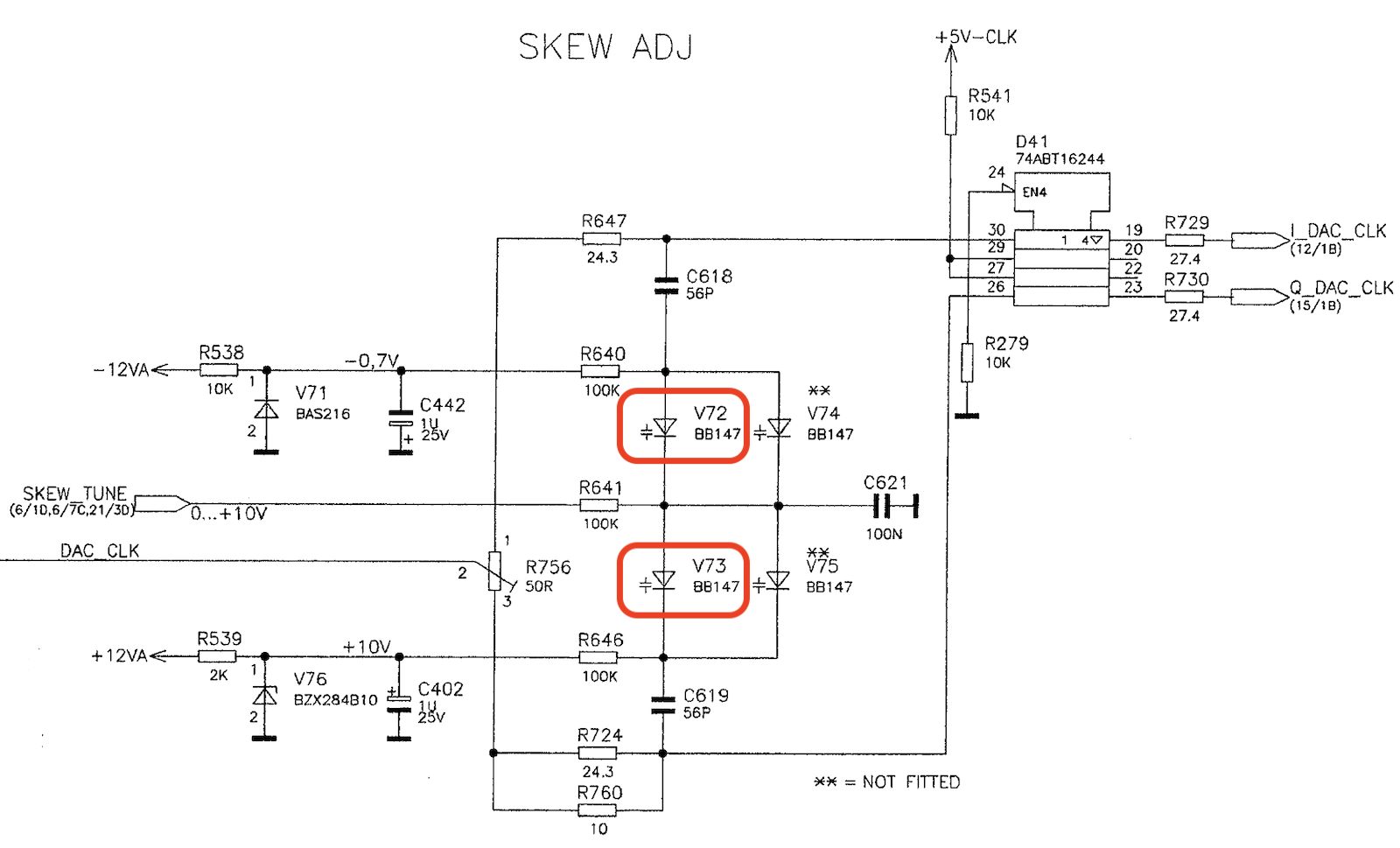
Starting with input signal DAC_CLK, the goal is to create I_DAC_CLK and Q_DAC_CLK that
can be moved up to 1ns ahead or behind the other. Signals can be delayed by sending them through
an R/C combo. Since we need a variable delay, we need a way to change the value of either the R
or the C. A varactor or varicap diode is exactly that kind of device: its capacitance changes
depending on the reverse bias voltage across the diode.
Static input signal SKEW_TUNE comes from a DAC. It goes to the cathode of one varicap and the
anode of the other. When its voltage increase, the capacitance of those 2 diodes moves in opposite
ways, and so does the R/C delay along the I and Q clock path.
A BB147 varicap
has a capacitance that varies between 2pF and 112pF depending on the bias voltage.
Capacitances C168 and C619 prevent the relatively high bias voltages from reaching the digital signal path.
Does the circuit work? Absolutely!
The scope photos below show the impact of the skewing circuit when dialed to the maximum in both directions:
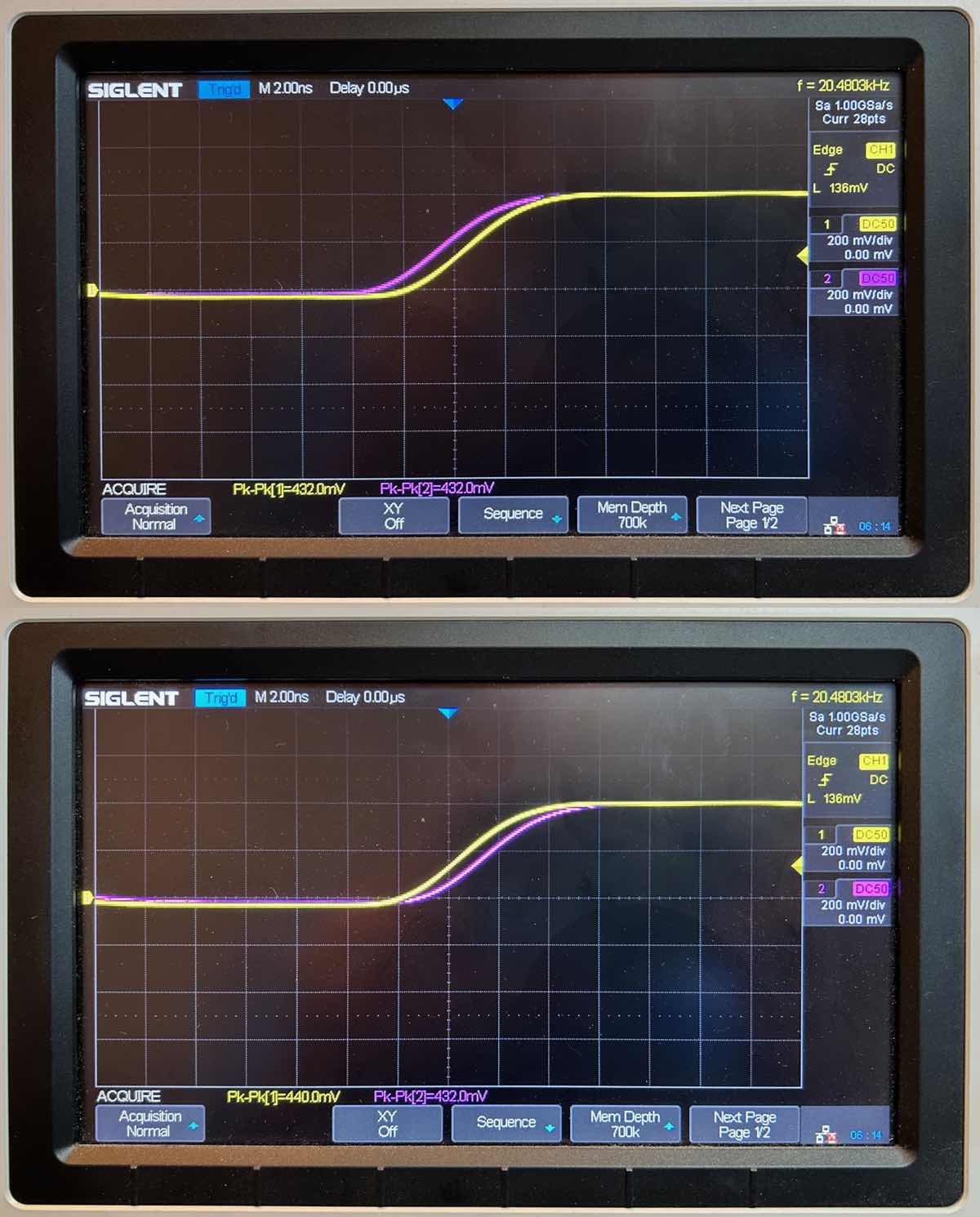
With a 2ns/div horizontal scale, you can see a skew of ~1ns either way.
Variable Gain Amplifier
The analog signal path starts at the DAC and then goes through the anti-aliasing filters, an output section that does amplification and attenuation, and finally the output connector board.
It is common for signal generators to have a fixed gain amplification section and then some selectable fixed attenuation stages: amplifiers with a variable gain and low distortion are hard to design. If you need a signal amplitude that can’t be achieved with one of the fixed attenuation settings, one solution is to multiply the signal before it enters the DAC to reduce the output amplitude, though that’s at the expense of losing some of the dynamic range of the DAC.
This is not the case for the AMIQ: while it can use a signal path that only uses fixed amplification and attenuation stages, it also offers the intriguing option to send the analog signal through an analog multiplier stage:
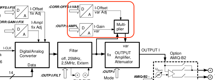
If we zoom down from the system diagram to the block diagram, we can see how the multiplier/variable
attenuator sits between the filter and the output amplifier, with 2 control input signals:
AMPL_CNTRL and OFFSET. This circuit exists twice, of course, for the I and the Q channel.
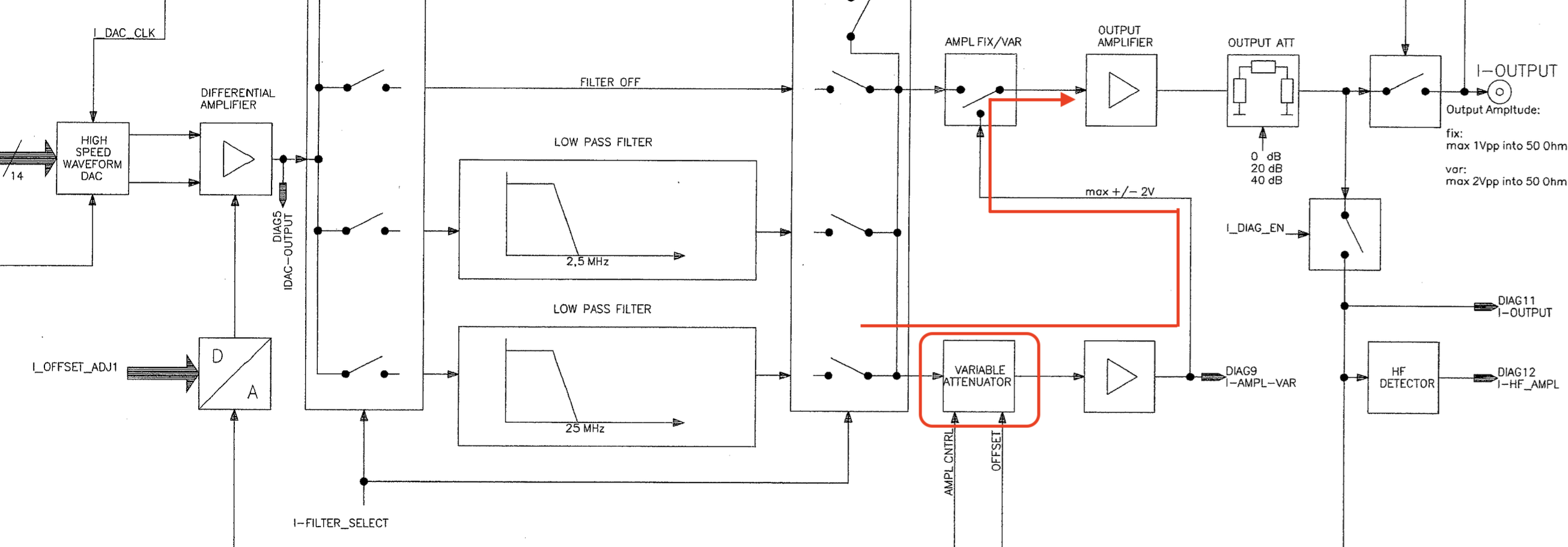
Let’s check out the details!
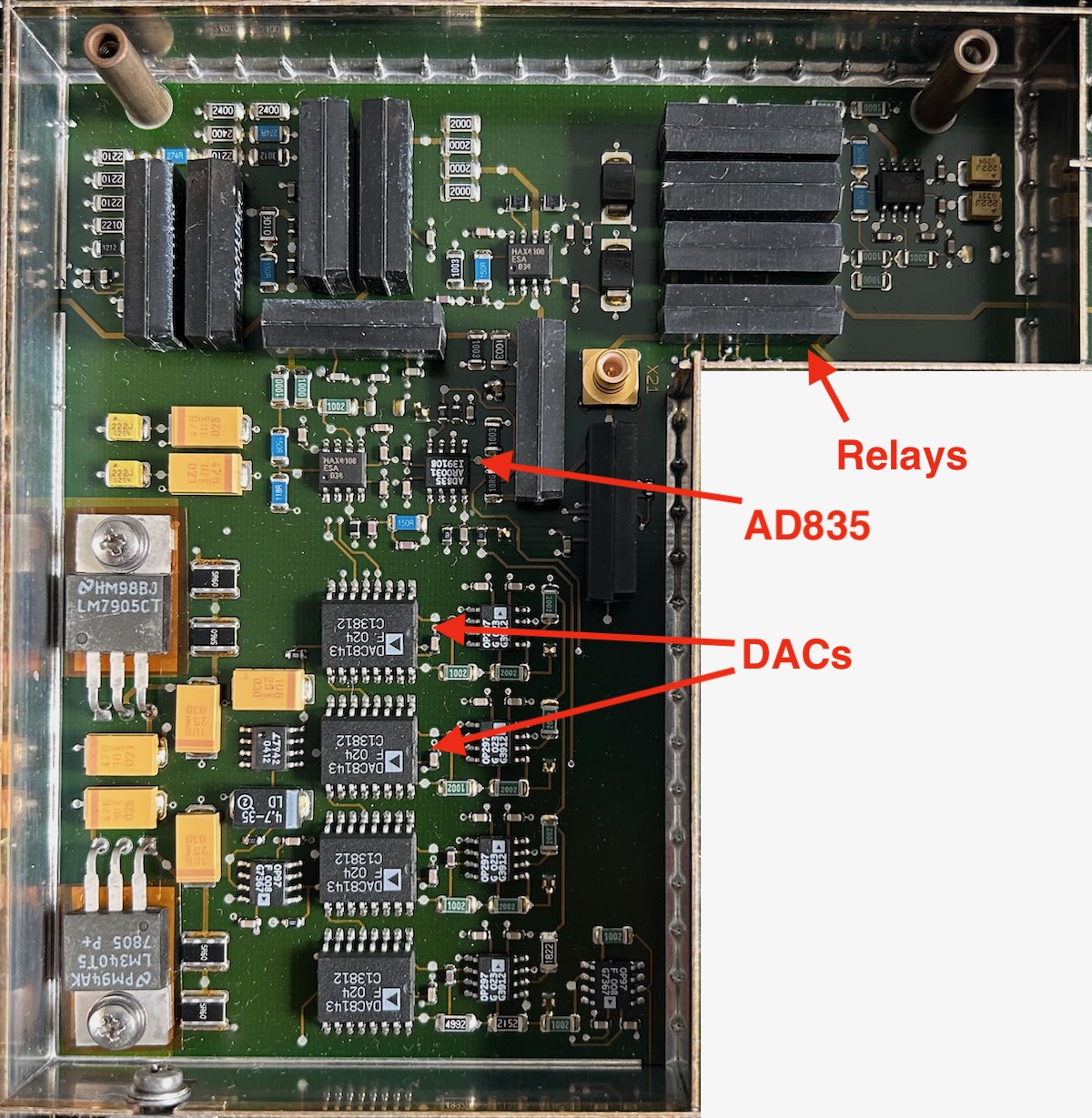
The heavy lifting of the variable gain amplifier is performed by an Analog Devices AD835 250 MHz, Voltage Output, 4-Quadrant Multiplier, a part from their Analog Multipliers & Dividers catalog.
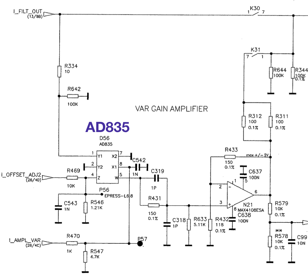
It’s a tiny 8-pin device that calculates W = (X1-X2) * (Y1-Y2) + Z. In low volume, it will set you back $32 on Digikey.
In addition to the multiplication, you can set a fixed output gain by feeding back output W through a resistive
divider back into Z. For inputs less than 10 MHz, it has a typical harmonic distortion of -70dB.
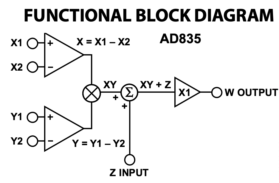
Analog Devices datasheets usually have a Theory of Operation section that explain, well, the underlying theory of operation. The AD835 has such a section as well, but it doesn’t go any further than stating that
the multiplier is based on a classic form, having a translinear core, supported by three (X, Y, and Z) linearized voltage-to-current converters, and the load driving output amplifier.
I have no clue how the thing works!
In the case of the AMIQ, X2 and Y2 are strapped to ground, and there’s no feedback from
W back into Z either which reduces the functionality to: W = FILTER_OUT * AMPL_VAR + OFFSET.
AMPL_VAR and OFFSET are static analog values that are each created by a 12-bit DAC8143,
just like many other analog configuration signals.
It’s almost shame that this powerful little device is asked to perform such a basic operation.
While researching the AD835, somebody pointed out the AD8310, another interesting speciality chip from Analog Devices. It’s a DC to 440 MHz, 95dB logarithmic amplifier, a converter from linear to logarithmic scale basically.
Discovering little gems like this is why I love studying schematics of complex devices.
Internal Diagnostics
The AMIQ has a set of 15 internal analog signal to monitor the health of the device. Various meaningful signals are gathered all around the signal generation board and measured at power up to give you that dreaded Diagnostic Check Fail message.
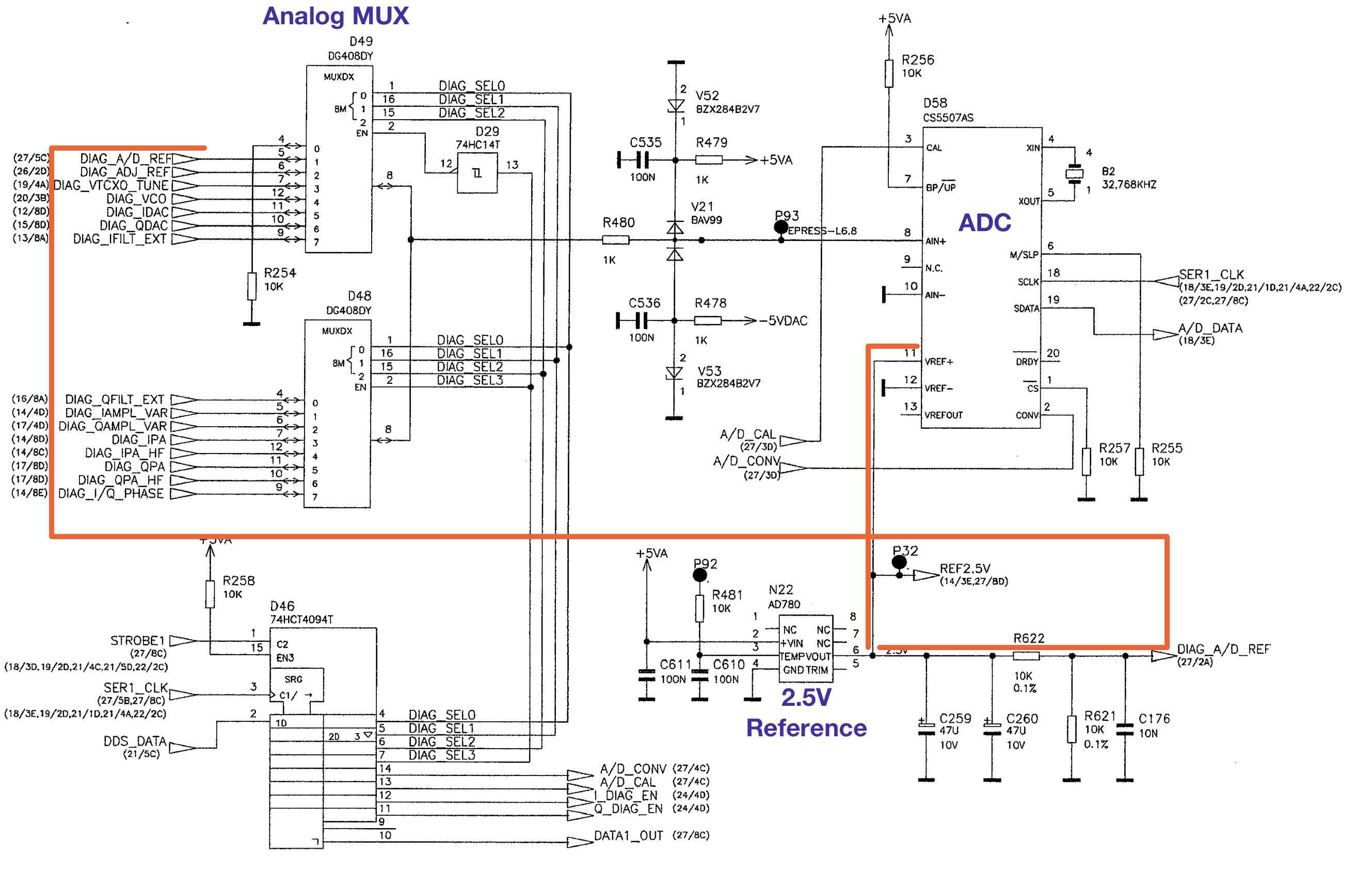
The circuit itself is straightforward: 2 8-to-1 analog multiplexers feed into a CS5507AS 16-bit AD converter. It can only do 100 samples per second, but that’s sufficient to measure a bunch of mostly static signals.
Like many other devices, the measured value is sent serially to one of the FPGAs.
The ADC needs a 2.5V reference voltage. It’s funny that this reference voltage also goes to the analog multiplexers as one one of the diagnostic signals. One wonders what the ADC returns as a result when it tries to convert the output of a broken reference voltage generator.
There are a bunch of circuits in the AMIQ whose only purpose is generating diagnostic signals. Here’s a good example of that:
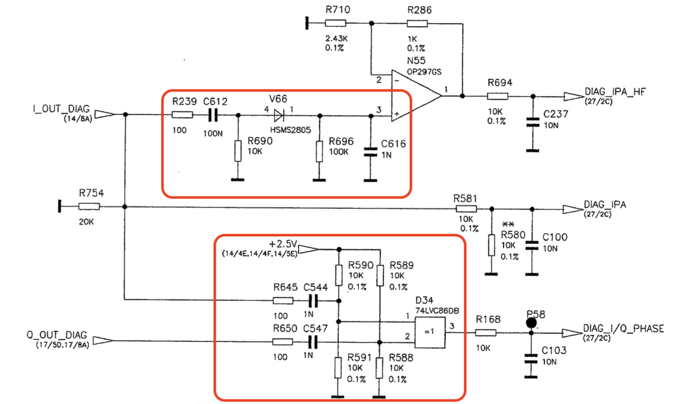
I_OUT_DIAG and Q_OUT_DIAG are the outputs after the attenuator that will eventually end
up at the connectors. The circuit in the top red square is a signal peak detector, similar
to what you’d find in the rectifier of a power supply. It allows the AMIQ to track the output
level of signals with a frequency that is way higher than the sample rate of the ADC.
The circuit in the red rectangle below performs a digital XOR on the analog I and the Q signals and then sends it through a simple R/C low pass filter. I think that it allows the AMIQ to check that the phase difference between the I and Q channel is sensible when applying a test signal during power-on self-test.
Efficient Distribution of Configuration Signals
The AMIQ signal board has hundreds of configuration bits: there are the obvious enable/disable or selection bits, such as those to select between different output filters, but the lion’s share are used to set the output value of many 12-bit DACs.
Instead of using parallel busses that fan out from an FPGA, the AMIQ has a serial configuration scan chain. Discrete 8-bit 74HCT4094 shift-and-store registers are located all over the design for the digital configuration bits. The DAC8134 devices have their own built-in shift register and are part of the same scan chain.
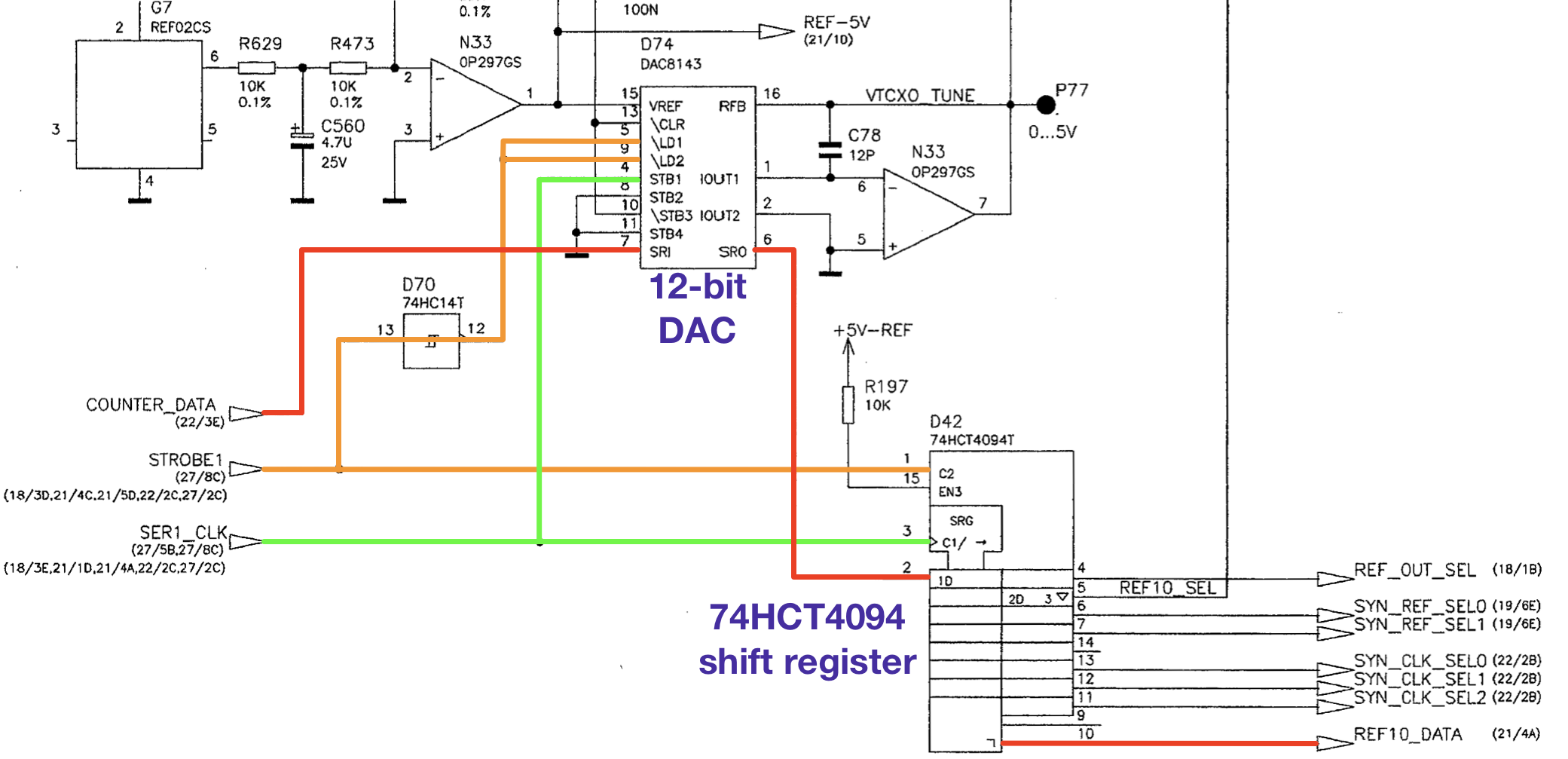
The schematic above is an example of that. The red scan chain data input goes through the VTCXO_TUNE DAC, then
the 74HCT4094 after which it exist to some other page of the schematics.
Conclusion
Around the late nineties, test equipment companies started to stop adding schematics to their service manuals, but the R&S AMIQ is a nice exception to that. And while the device already has a bunch of FPGAs, most of the components are off-the-shelf single-function components. Thanks to that, the AMIQ is an excellent candidate for a deep dive: all the information is there, you need to just spend a bit of effort to go through things. I had a ton of fun figuring out how things worked.
References
Rohde & Schwarz documents
- R&S - IQ Modulation Generator AMIQ
- R&S - AMIQ Datasheet
- R&S - AMIQ Operating Manual
- R&S - AMIQ Service Manual with schematic
Various application notes
- R&S - Floppy Disk Control of the I/Q Modulation Generator AMIQ
- R&S - Software WinIQSIM for Calculating I/Q Signals for Modulation Generator R&S AMIQ
- R&S - Creating Test Signals for Bluetooth with AMIQ / WinIQSIM and SMIQ
- R&S - WCDMA Signal Generator Solutions
- R&S - Golden devices: ideal path or detour?
- R&S - Demonstration of BER Test with AMIQ controlled by WinIQSIM
Other AMIQ content on the web
- zw-ix has a blog - Getting an Rohde Schwarz AMIQ up and running
- zw-ix has a blog - Connecting a Rohde Schwarz AMIQ to a SMIQ04
- Bosco tweets
DDS Clock Synthesis
- MT-085 Tutorial: Fundamentals of Direct Digital Synthesis (DDS)
- How to Predict the Frequency and Magnitude of the Primary Phase Truncation Spur in the Output Spectrum of a Direct Digital Synthesizer (DDS)
Related content