HP 16500A Logic Analyzer Teardown
This is the only the first part of what will probably be a series of blog posts. No earth-shattering revelations in here, just taking the thing apart and looking at the datasheet of some of the chips…
- Introduction
- Safety First
- Powering it up
- Disassembly Tools
- Tearing Down the Logic Analyzer
- Identifying Components inside HP Products
- Main Controller Board Overview
- CPU System Components
- Display Hardware Architecture
- Communication Devices
- HP Human Interface Link Host Controller
- More Coming Up…
- References
Introduction
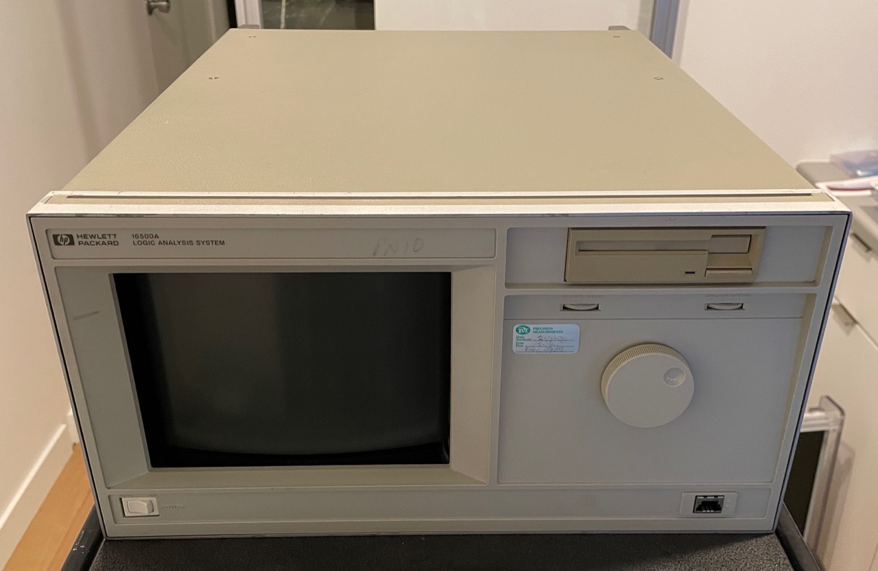
I recently became the proud owner of an HP 16500A logic analyzer for the low low price of $20.
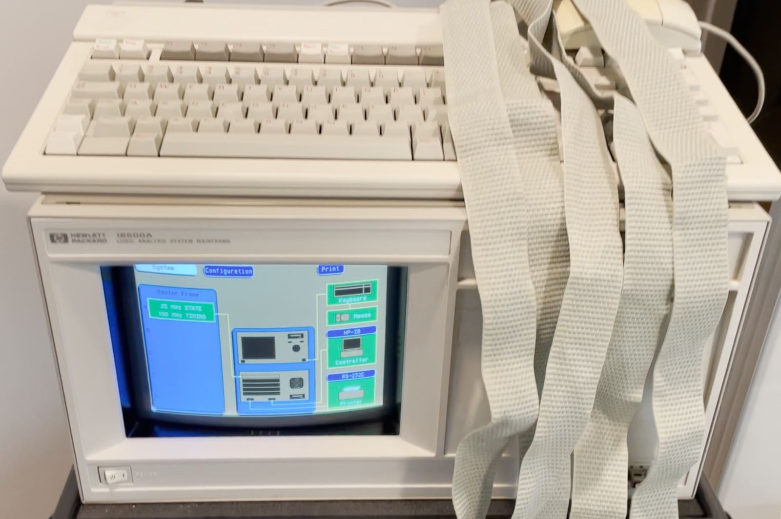
Or better, I’m now the owner of two HP 16500A logic analyzers, because the seller had a whole pallet of them, and when you have a spare, you can afford to take more risks while experimenting with them. The second one even came with an HP keyboard and mouse.
$20 is obviously an exception, but these machines aren’t expensive in general: you should be able to find one for $100 on eBay without much effort, though expect to add another $75 for shipping, because these things are big and heavy.
The 16500A is a mainframe design, with a 6-slot backplane that contains CPU controller board and 5 additional slots for various plug-in measurement cards. My 2 units came with an HP 16510A: an 80 channel 25MHz/100MHz digital acquisition card with a 4K acquisition depth, but higher performance cards exist.
The logic analyzer functionality itself is not particularly useful for me: I never need to record that many channels in parallel, the acquisition depth is pathetic, the maximum sample rate is too low, and it’s not trivial to get data of the machine for later analysis, because you need either use a non-standard floppy drive or the GPIB interface. It’s also a huge, heavy beast that’s impractical to move around on a bench, and you can’t even disconnect the unwieldy measurement cables that you don’t use.
In short, this unit is worse in almost any respect than the Saleae Logic Pro 16 that I use at work. It also explains the low cost: there are much better alternatives. Its successor, the 16500B, uses a much faster hard disk to store the main software, and the 16500C has support for an Ethernet connection.
But it’s always fun to take a vintage piece of electronics apart just for the sake of it, learn about its special features, and maybe come up with some interesting future project ideas?
So in this blog post, I’ll take whole thing apart and try to figure out how what makes it tick.
Safety First
Before opening and working on this machine, it’s import talk about safety:
WORKING ON SOMETHING LIKE THIS COULD KILL YOU.
There, I’ve said it. So, please, if you’re not familiar with devices like this, just read this blog for entertainment and don’t try to reproduce my results. If you decide to do it anyway, you do so at your risk, and take a number of basic precautions:
- Read the HP 16500A service manual. It is authoritative, unlike the scrappy blog of some electronics hobbyist.
- Unplug the AC power cable before you start going at it with a screw driver.
- Wait 5 minutes after unplugging the AC power cable: the power supply unit of an HP 16500A has a lot of large capacitors and does not have bleeder resistors to quickly discharge them after power is removed.
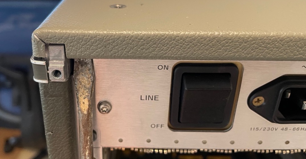
- The power switch on the front panel is not in fact a power switch. It merely puts the device in a standby low(er) power state. There is a real power switch at the back of the device.
- The HP 16500A power supply unit creates 120V DC to power the CRT module. Most power supply units only create relatively low DC voltages, this one does not. Be extra careful.
- CRT tubes require very high voltages. I’m not totally sure about this one, but the CRT schematic has annotations of 800V.
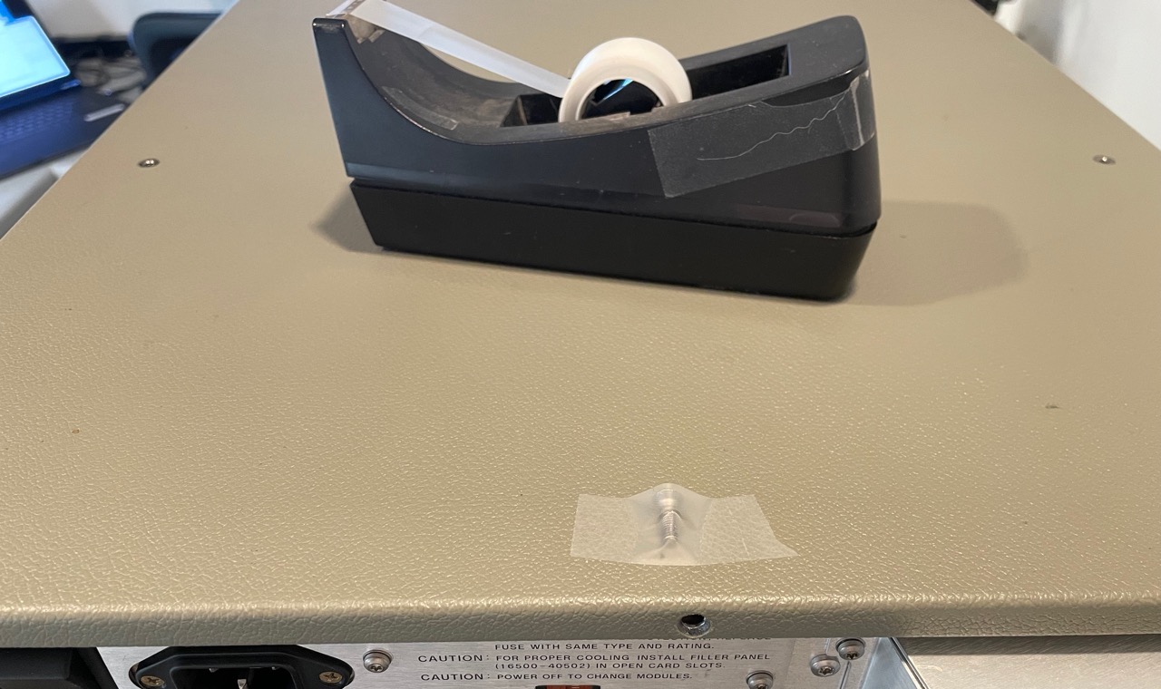
- Be extra careful about dropping screws. There are a lot of them. If one drops, get it out before moving on to the next one. You don’t want specialty fireworks due to a screw induced short circuit!
- If you want to switch on the device while the covers are removed, tape some cardboard on top of the CRT unit to prevent accidentally touching the high voltage parts.
- Never do any measurements inside the bowels of the CRT module when it’s powered on. Sony provided a lot of measurement test points on the outside PCBs. There is absolutely no need to get inside.
- Have a clean workspace. My bench is usually a horrible mess, but I unclutter it for projects like this.
Powering it up
Taking pictures of running CRT screen is a pain, and they generally look terrible. Just assume that whatever you see here will look much better in real life.
After powering up the device, you should see a boot screen like this:
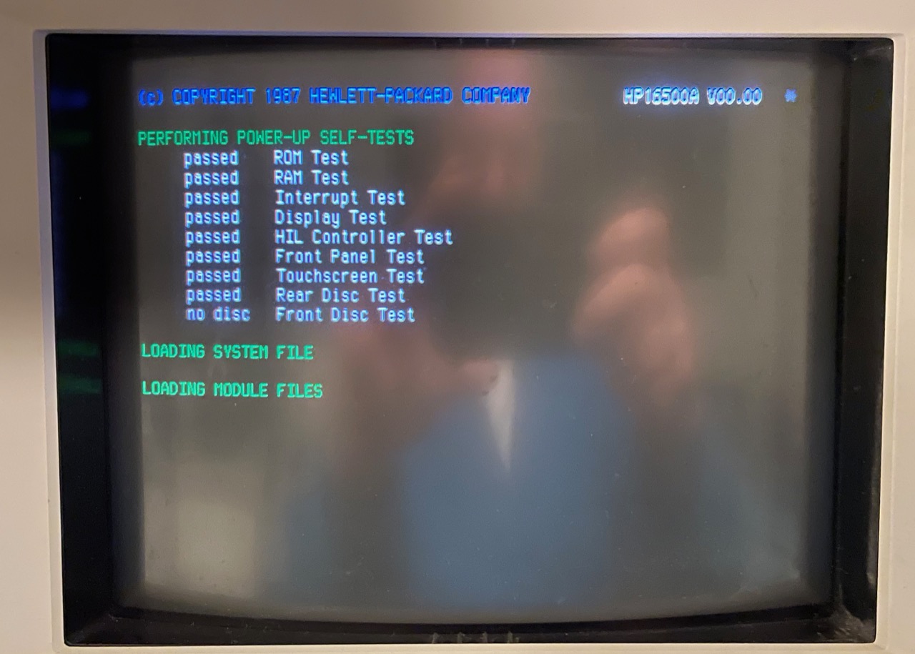
The HP 16500A has 2 floppy drives, one in the front and one in the back, and other than some boot EPROMs, it has no other means to store its system software. So in practice you’ll always keep a system disk in the rear floppy drive. The floppy drive is not compatible with standard drives from the mid eighties: it’s a special 600RPM Sony drive.
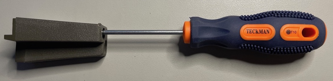
Disassembly Tools
I’ve opened plenty of test and measurement devices before, and so far, all I needed where regular flat-head, Philips, and hexagonal screw drivers. Not so for the HP16500A: it uses Torx 10, 15, and 20 screws everywhere. And even if you already have some Torx heads that plug into a generic screwdriver, you still won’t be able to open up the logic analyzer.
That’s because you can’t remove any of the 4 enclosing side panels without removing 4 feet at the back and each of those 4 feet has a Torx 10 screw sunken deep inside a narrow hole.
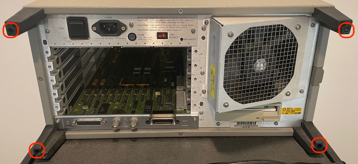
The only way to get to it was with a dedicated, narrow, Torx screw driver, not a generic one with exchangable heads.
One of the benefits of having many projects going on in parallel is that you can switch to something else while an order for tools is on its way.

If you’re going the route of buying a set, do yourself a favor and buy security Torx screwdrivers: they fit in the same holes are regular ones, but have an additional axial hole for security Torx screws, which will allow you, hypothetically, to remove somebody’s Ring camera from their front door.
Tearing Down the Logic Analyzer
If you’re not interested in knowing exactly which screws to unscrew or connector to unplug, click here to fast-forward to the next section.
Section VI of the service manual explains how to take the whole device apart to replace pretty much all larger components in case of failure. It’s not particularly difficult to open it up, but I have a bit of tradition of showing too much of the disassembly process than too little, and I’m not going to stop that here.
Remove plug-in cards and empty slot covers
Let’s start with that, because it’s easy and all these annoying cables won’t be in the way anymore.
Note that it’s not possible to remove the CPU system card at the bottom, because not only does the left bottom foot blocks it from sliding out, but also because a few flat cables, accessible after removal of the bottom panel, must be unplugged first.
Here is the removed HP 16510A acquistion card:
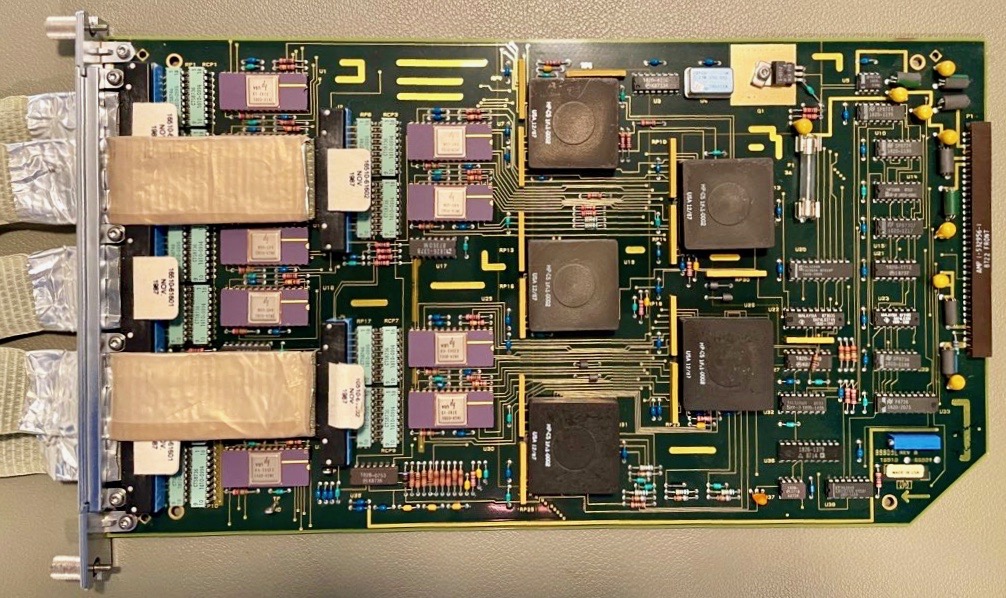
These 5 heatsinks probably cover some custom ASICs, and are thus a bit of dead-end. I’ll leave them be.
Remove the 4 feet in the back
Yes, this is the same picture as above!
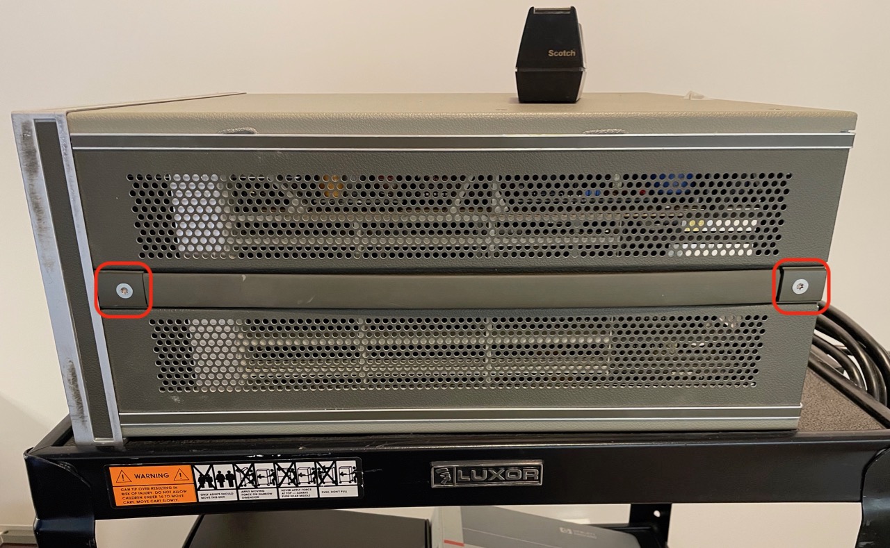
Remove 3 back panel retention screws
There isn’t a 4th screw, because one side panels has a carrying handle and screws to keep in place.
Whenever possible, I tape the screws to the place where they came from. That makes it much easier to assemble thing back together later.
Remove the handle from the side panel
A friend gave me rolling equipment cart. These things are amazing when you need to remove screws from all sides of a 40 pounds heavy box.
Remove the top and side panels
We can now remove the panels. You can slide each of the 4 panels from the front to the back, but there can be quite a bit of friction. The easiest way is to remove the top panel first.
Insert a flathead screwdriver in the gap between the back of the top panel and the back of the power supply unit and rotate the screwdriver until the panel comes loose.
Once loose, you can now easily slide out the top panel.
Since we already removed their back screws, the side panels can now slide out too.
You’ll be greeted by the following sight:
We can see a huge power supply, the front and back floppy drives, and the CRT unit.
All of these will come out soon.
Remove the bottom panel
Let’s turn the unit on its side and slide out the bottom panel.
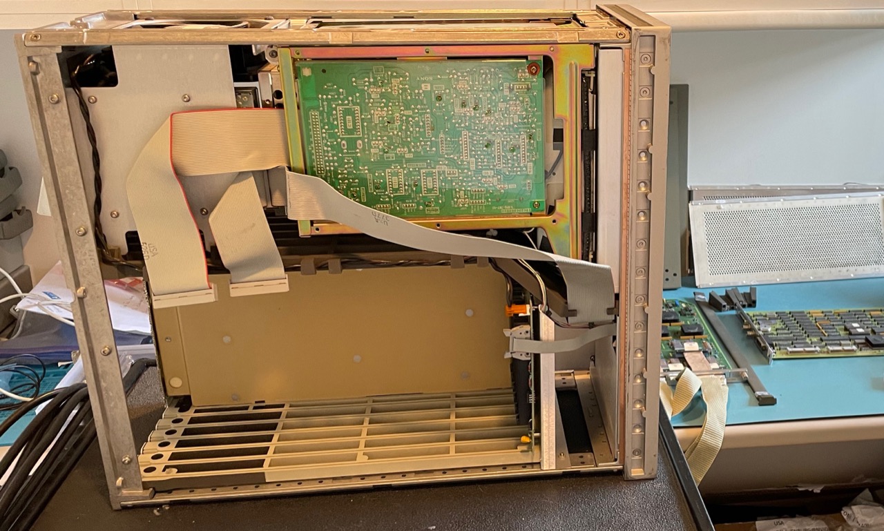
We now have access to all the main components.
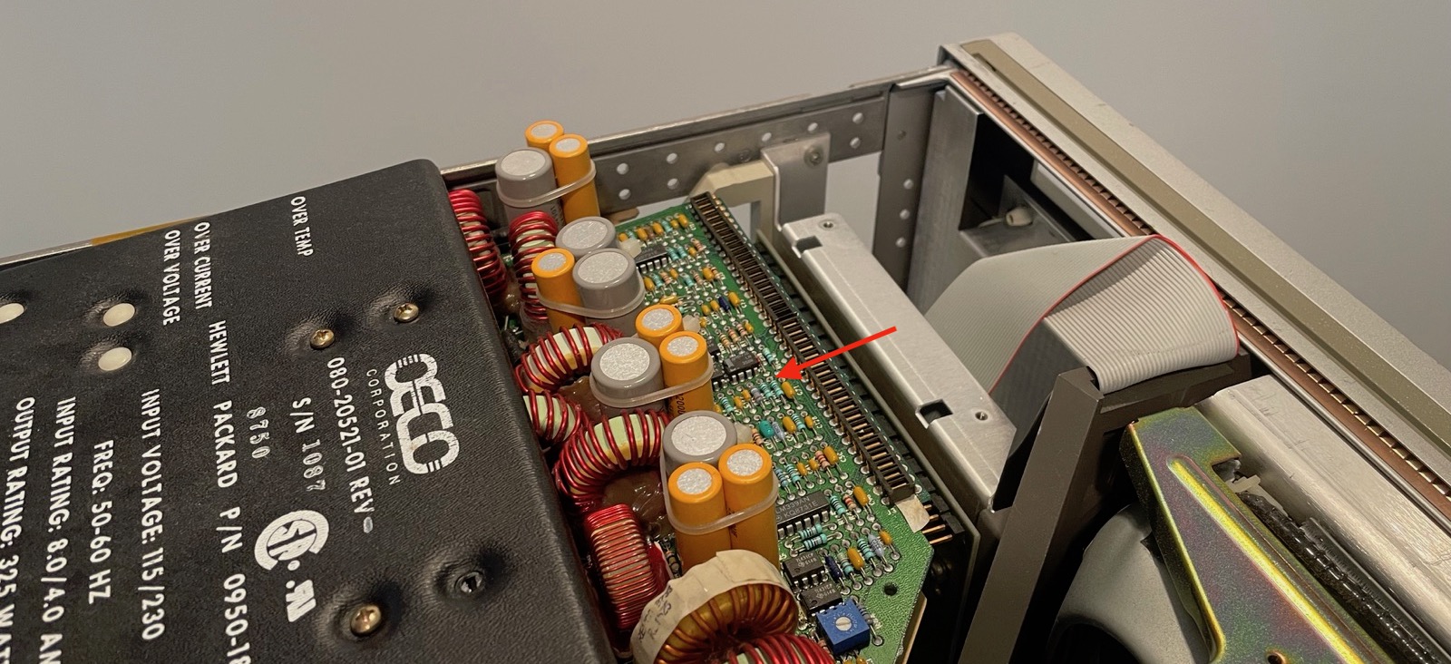
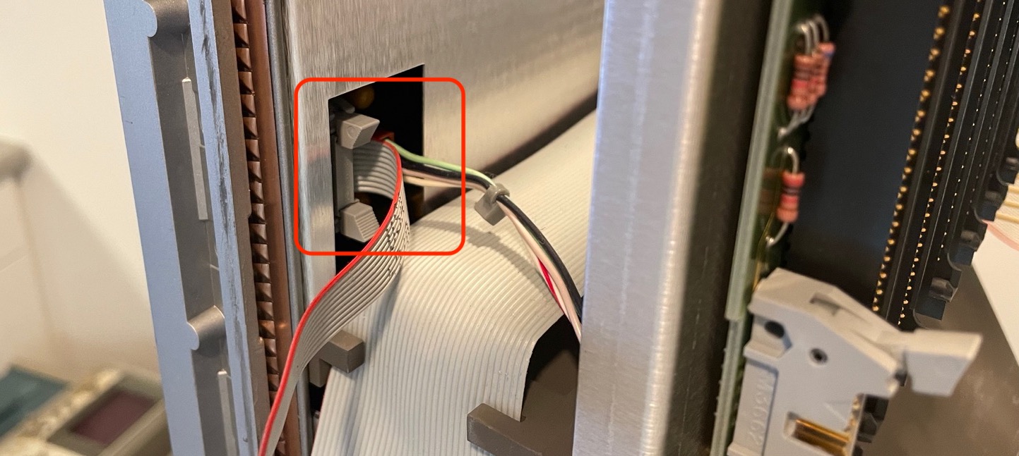
Remove the CPU controller board
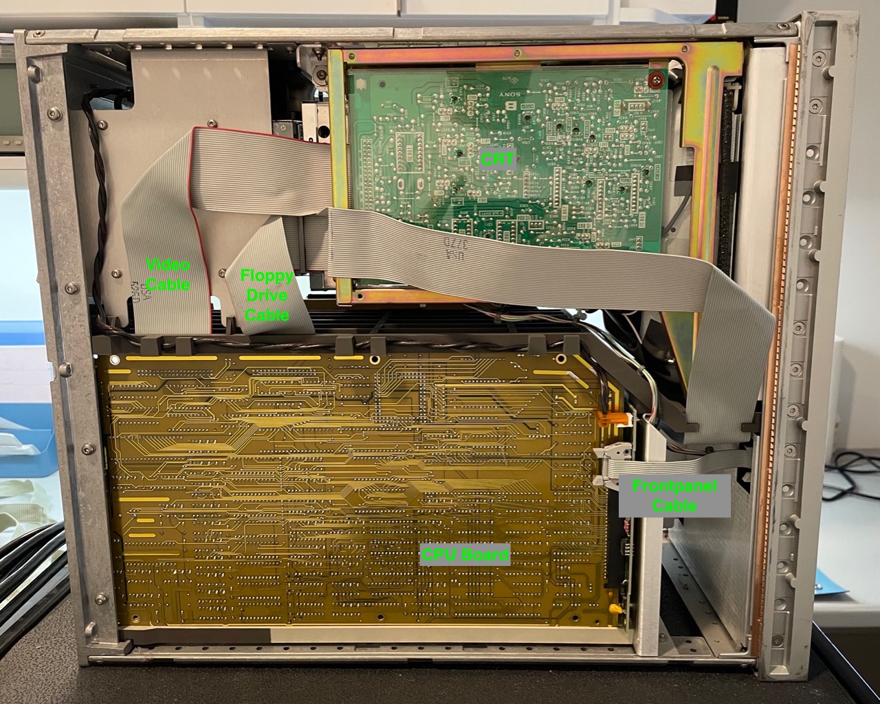
The video cable and the floppy drive cable are the only ones that connect directly to the CPU controller board. They’re much easier to unplug now that the back panel has been removed. I also unplugged the frontpanel cable and the orange cooling fan control cable, but that’s not necessary to remove the CPU board.
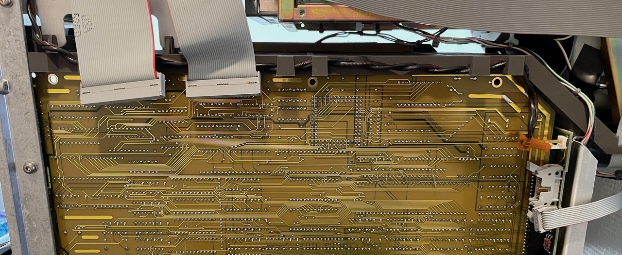
After removing the 2 screws in the back that secure the CPU board, we can slide it out. It looks really nice. Let’s put it aside for now. We’ll check it out more in detail later.
The whole chassis starting to look pretty empty already, but we’re far from being done!
Remove the front floppy drive
The front floppy drive blocks the exit of the power supply board. We can take it out by removing the 2 screws that are on the retaining bracket. (The second screw is hidden underneath the flat cable.)
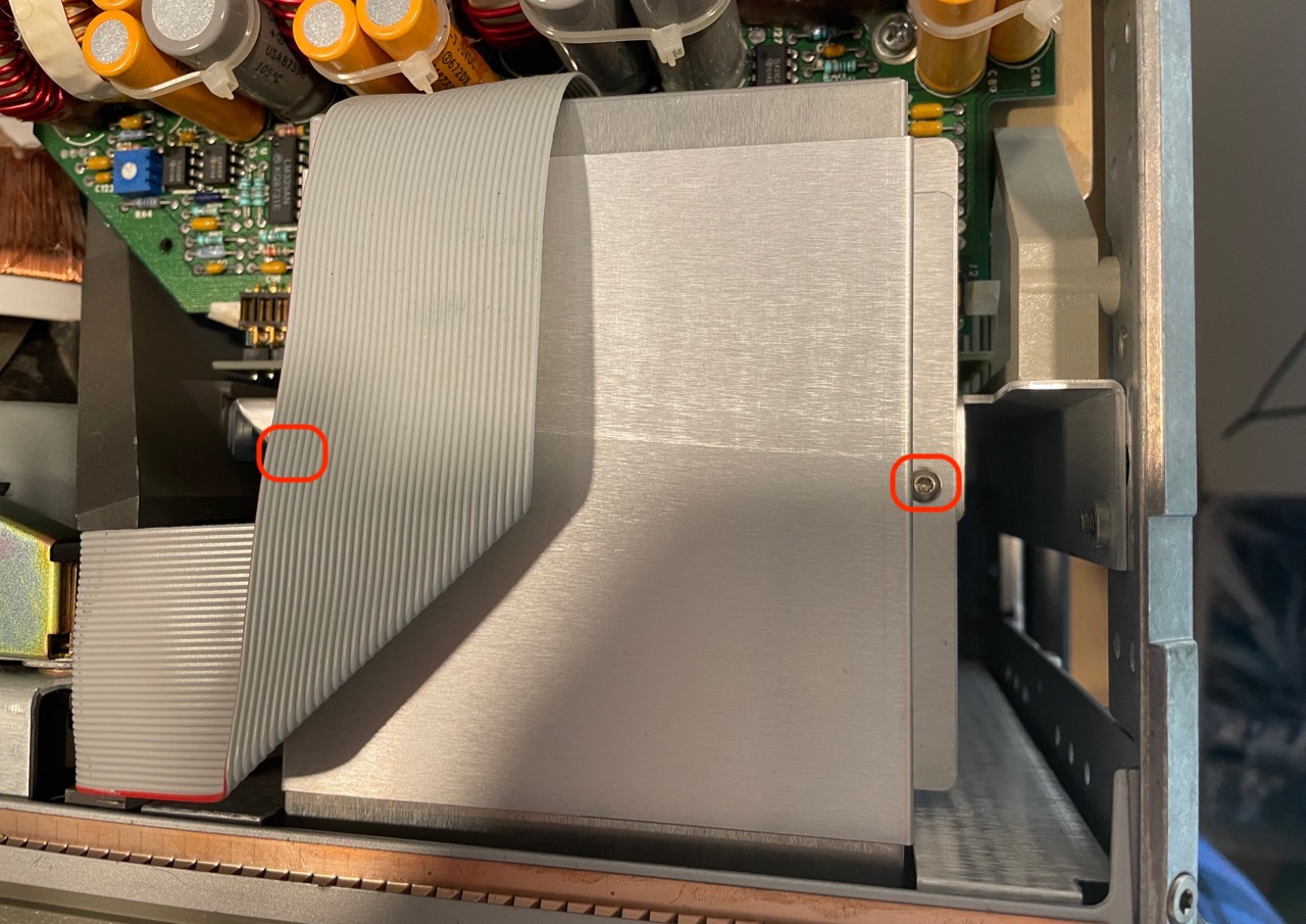
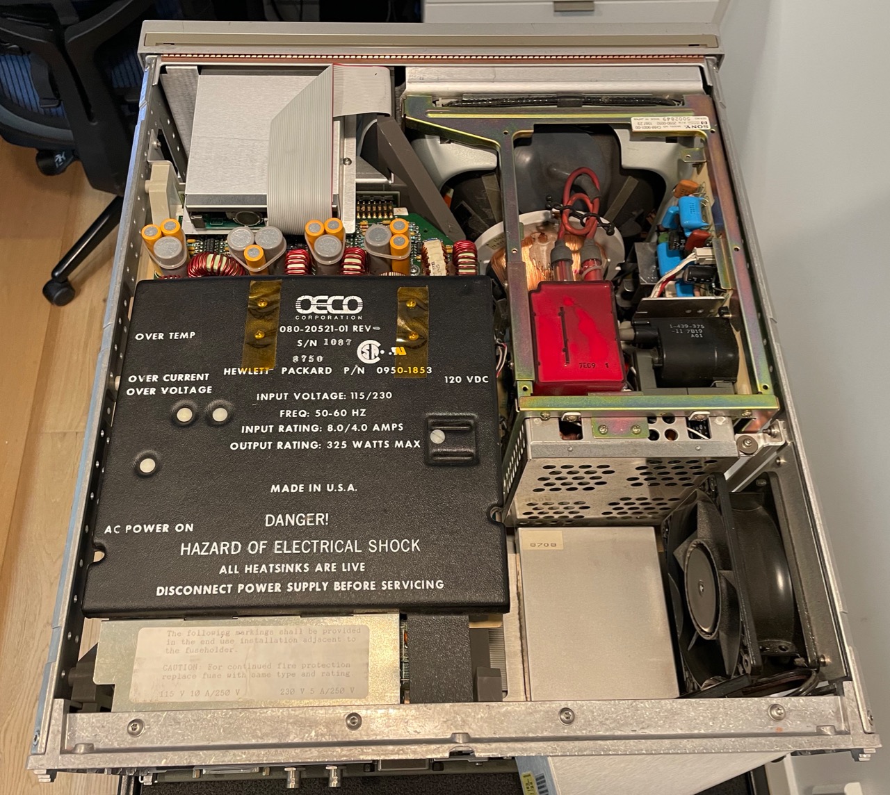
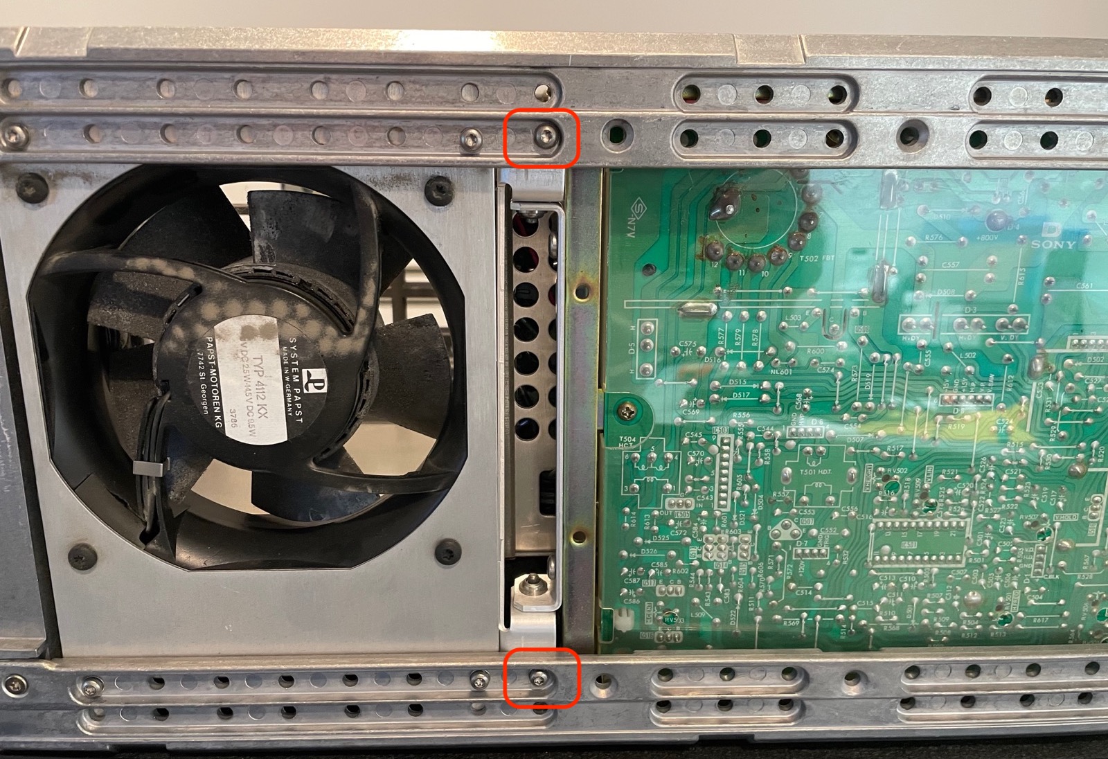
Remove the power supply unit
Getting the power supply unit out of the chassis is a bit more complicated.
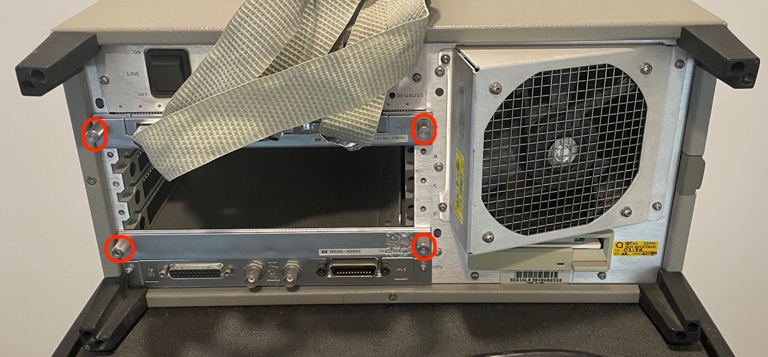
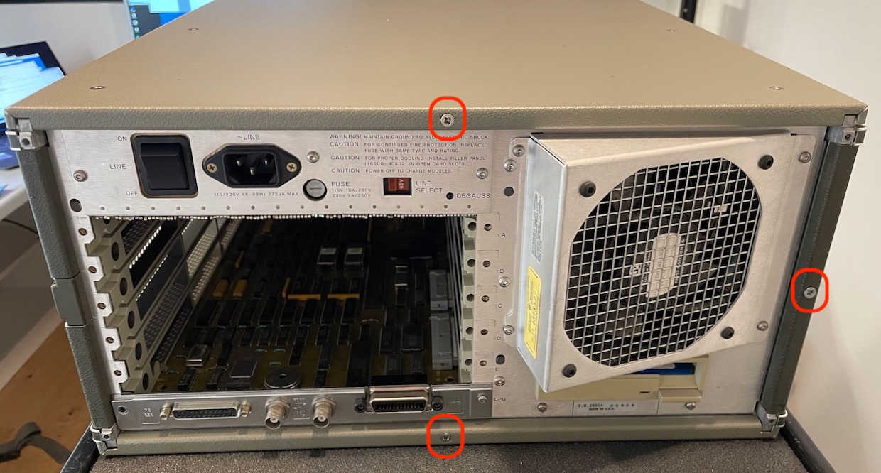
There’s a backplate screwed to the power supply with 3 screws:
On top, there are 2 screws that fix the power supply to the back frame, and 2 screws that are hidden below the black safety cover.
It’s not strictly necessary, but I also removed the 4 screws at the top to take off the safety cover itself, so that I could have a better look at the components of the power supply itself.
There is supposed to be Kapton tape over the 4 screws that hold the cover in place. Make sure to put that tape back when you reassemble the logic analyzer, because there’s a live voltage on those screws and they could make contact with the metal enclosure!!!
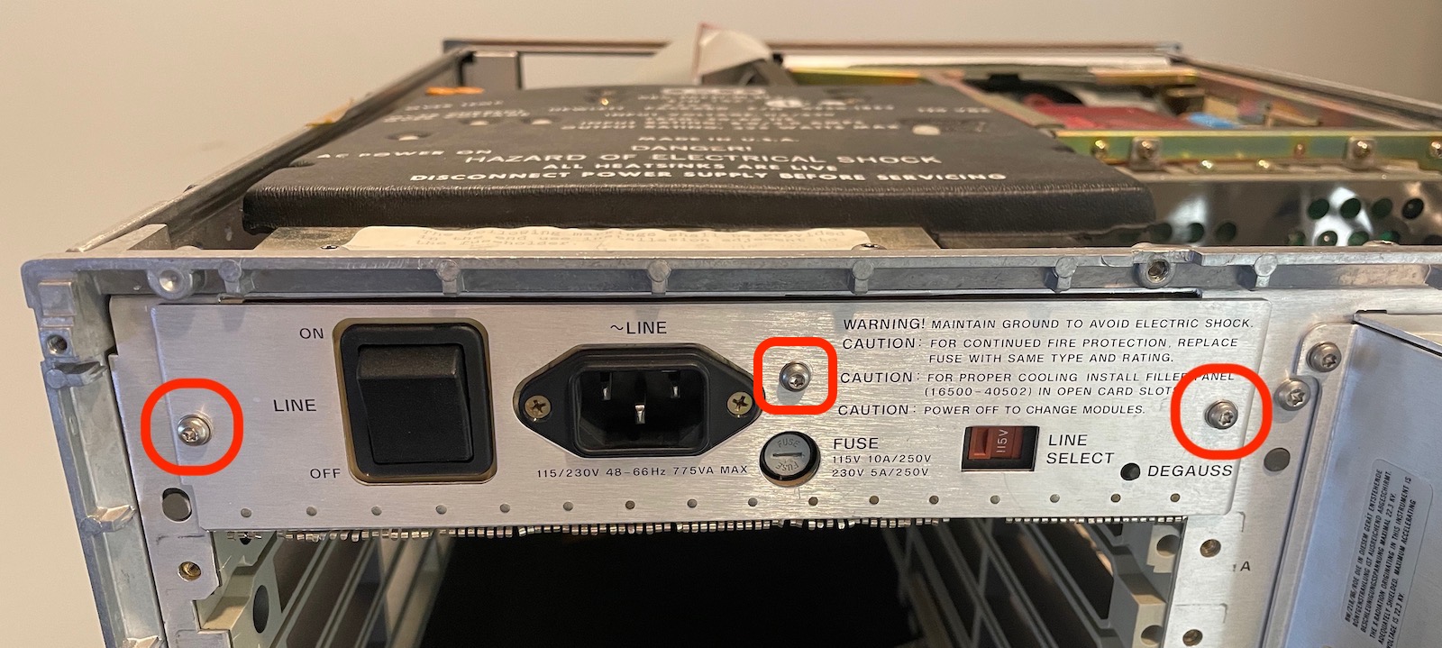
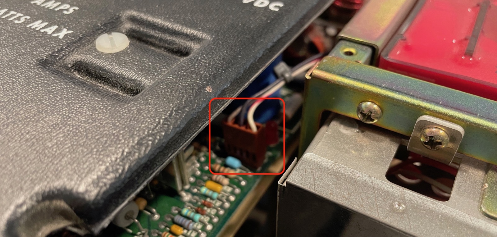
Now is also a good time to disconnect the CRT cable. It carries the 120V power for the CRT as well as the degauss signal that goes to a switch that’s located on the back of the power supply.
At first, the power supply cable seems surprisingly flimsy to carry the power of a CRT. But keep in mind that the thickness of a power cable is primarily determined by the current that must go through it, not the power. With a peak power of 60W, the supply voltage of 120V results in maximum current of only 0.5A. You don’t need a thick cable for that.
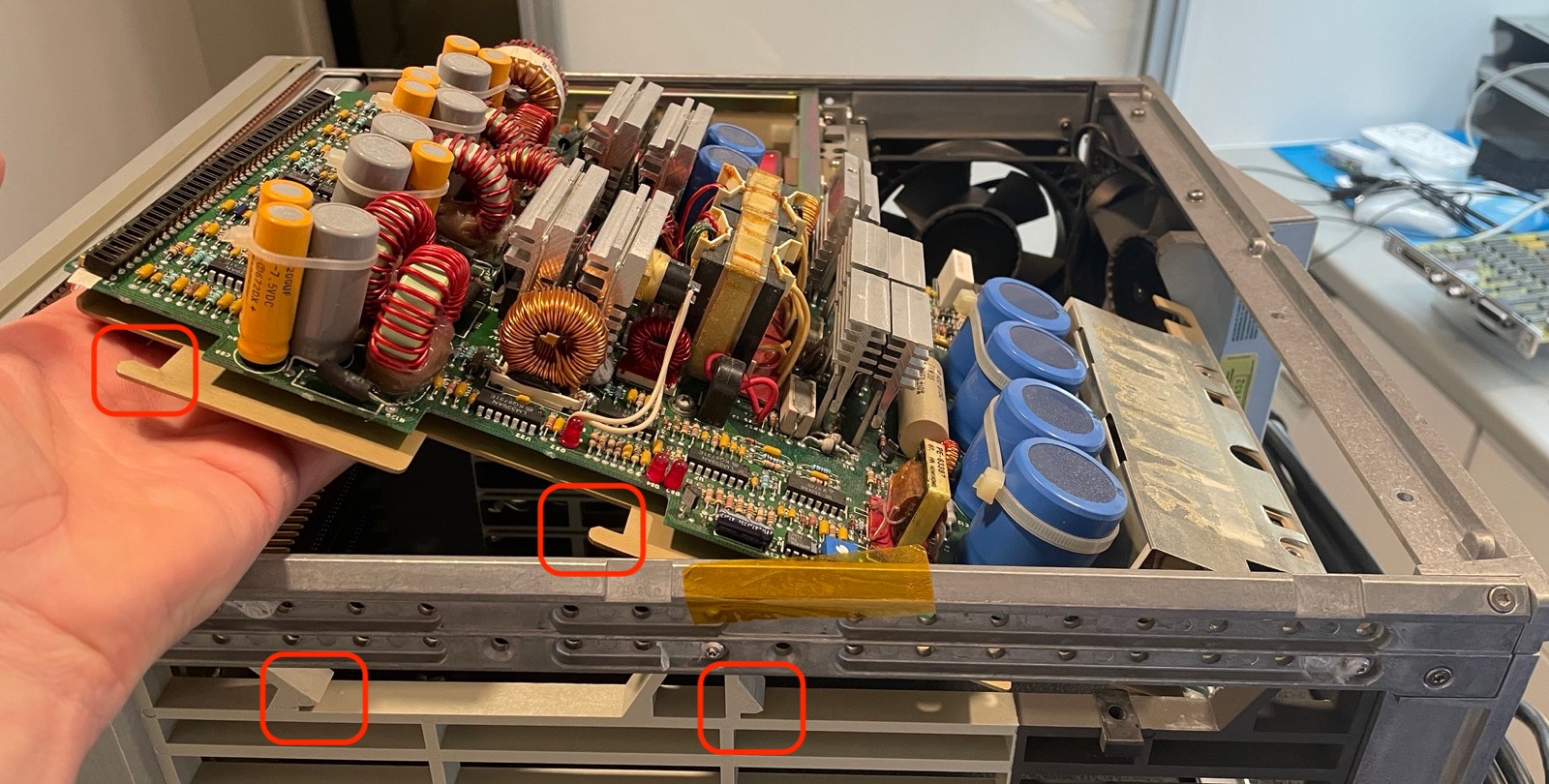
You can now disconnect the whole power supply from the backplane PCB by sliding it back by about a centimeter.
The power supply is held in place by teeth of a back plate the slide into plastic retaining slits. Once you moved the power supply back in the previous step, you should be able to lift the power supply out of the chassis. It’s a little bit tricky.
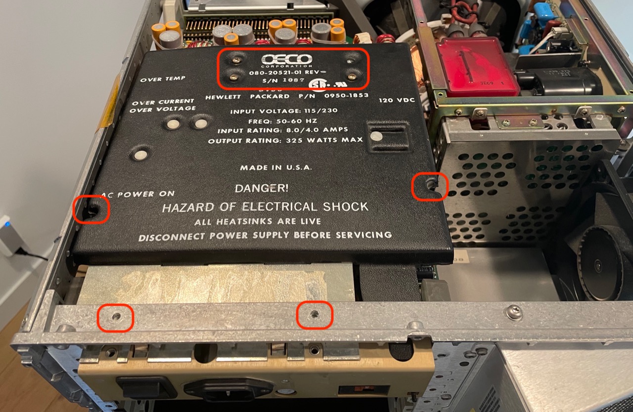
It’s a beast of a power supply that’s mounted on a heavy metal backplate.
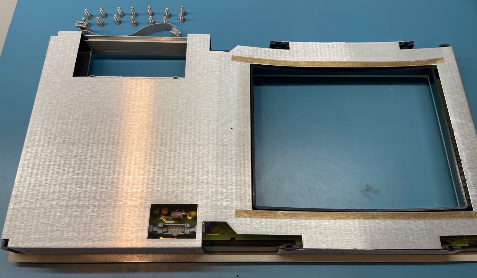
Front panel removal
The front panel contains a cool optical touch screen sensor. I definitely want to take a look at that, so off it goes.
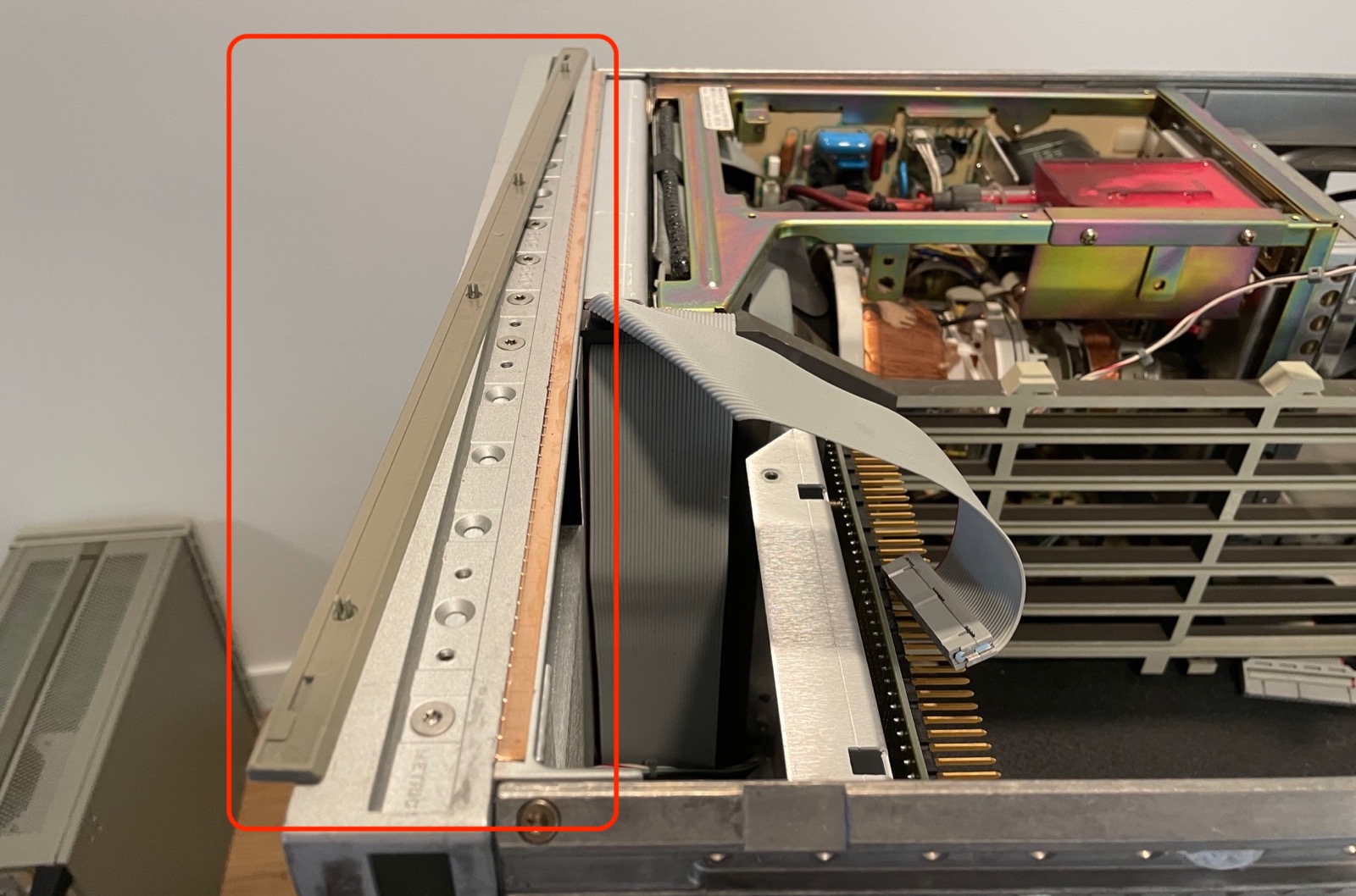
At the top of the front panel, there’s a gray strip that covers 7 screws. The strip can easily be removed with a narrow flat-head screwdriver. There are also 7 screws at the bottom.
After removing all 14 screws, the front panel is loose, but it will still be connected to the chassis with an interface controls flatcable to goes to the backplane PCB, and with a contrast and brightness cable that goes to the CRT. Unplug them too.
The front panel has metal shielding around it. You can simply remove it.
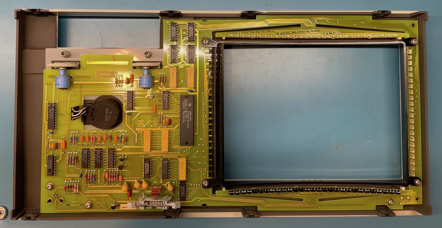
We can now have a good look at the internals of the user controls: rotary encoder, 2 potentiometers for brightness and contrast control, and, of course, rows and columns of LEDs and photodiodes for the optical touch screen. I love it!
I plan to do a deeper dive on this in a future blog post.
CRT Removal
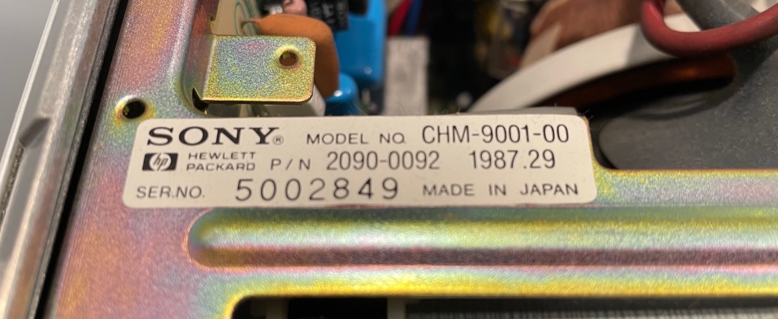
The final big item to remove is the CRT unit. It’s a Sony CHM-9001-00 with a Trinitron tube. This is probably the most interesting part of the whole logic analyzer. I’ve been experimenting with it and there’ll be definitely more to come on this one.
Remove the 4 screws that fix the CRT to the front top and bottom rails of the chassis:
The CRT claims a 9” active area, which seems about right.
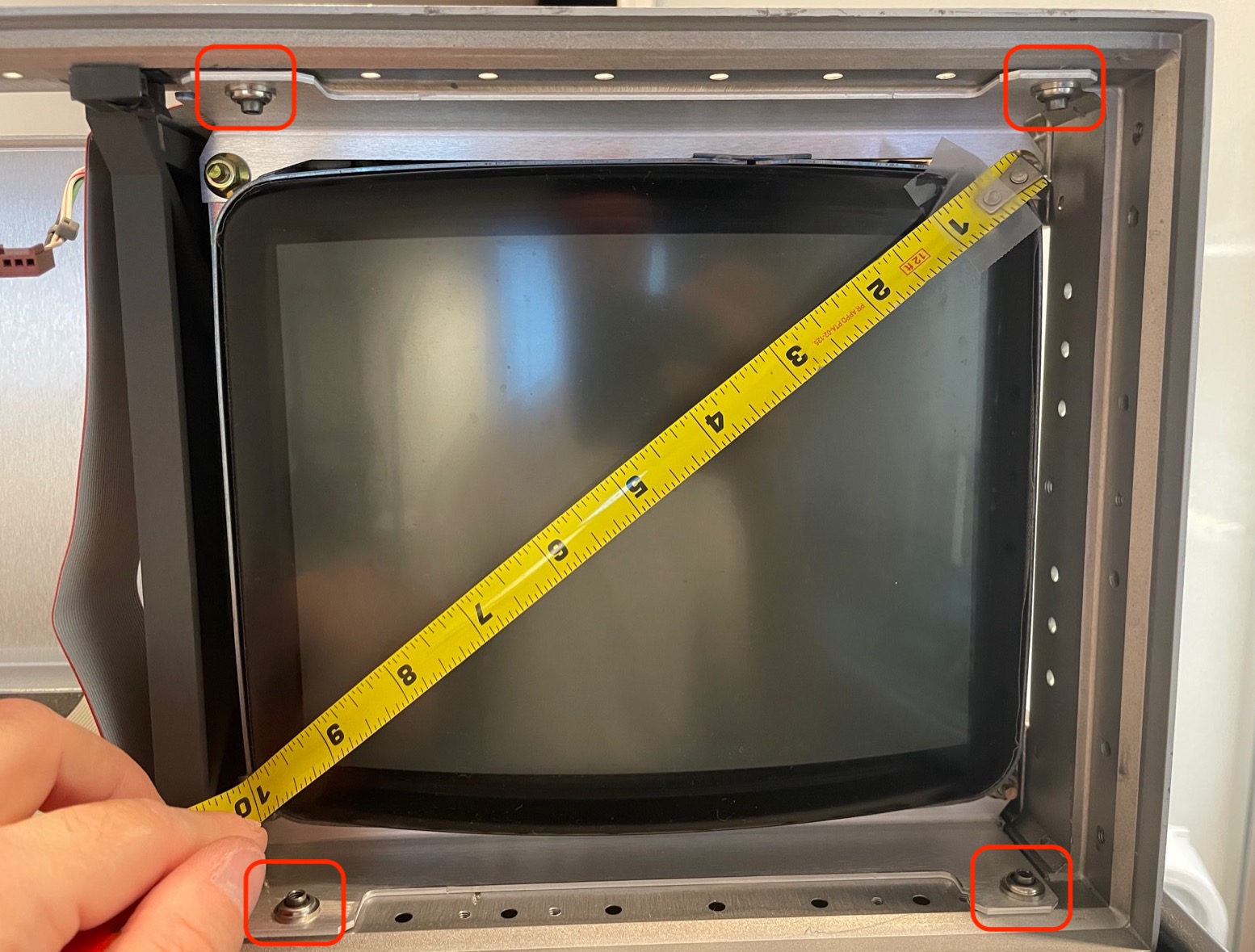
2 screws in the back fix the CRT unit to the side of the chassis.
The CRT unit can now slide out through the front. There were some black metal clips and grey plastic that was a little bit in the way, but after pushing those aside, it came right out.
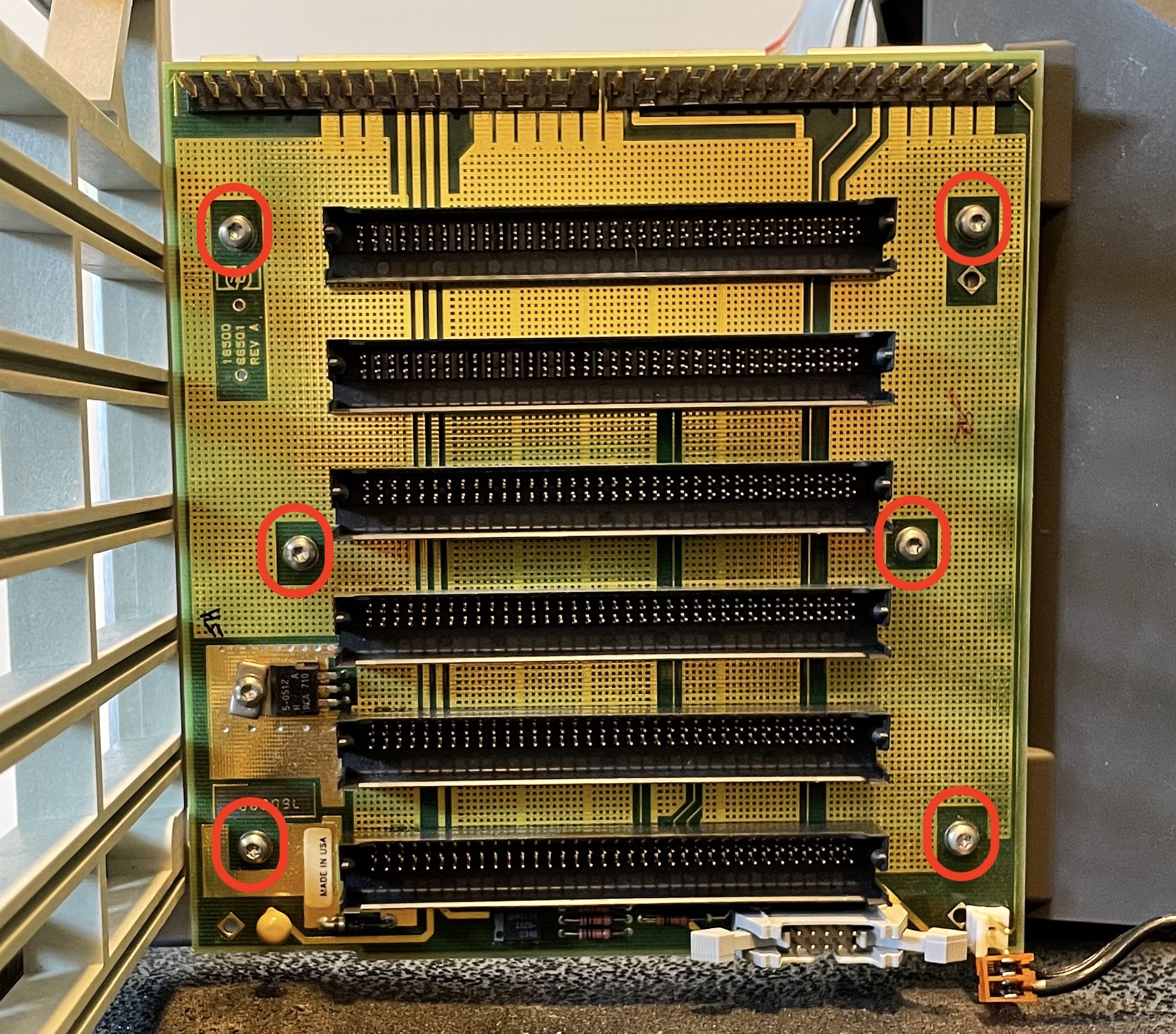
Backplane removal
I wanted to check out the backside of the backplane, so I removed it too. It has 6 screws.
All removed pieces together!
Here are all the items that have been removed, neatly organized next to each other.
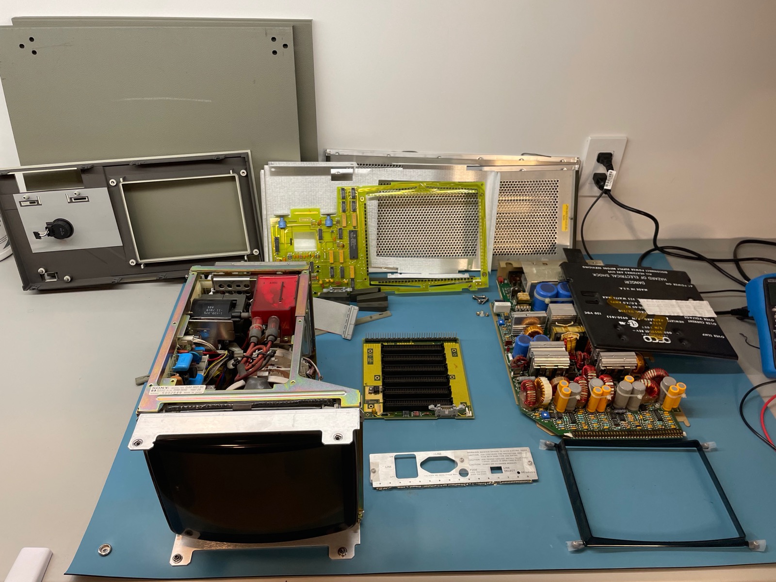
All that’s left in the chassis are the back floppy drive and 2 fans. It’s a whole lot lighter now!
Identifying Components inside HP Products
After taking everything apart, I wanted to identify some of the internal electrical components.
One useful piece of knowledge for those who want to do the same kind of exercise: there are at least 3 different types of HP part number identification:
- the generic part name of the original manufacturer. E.g. SN74LS374N is a piece of glue logic from the standard 74LS family.
-
the HP part number. Many components, even generic ones, were custom marked for HP with their unique number. And the generic name is sometimes dropped altogether. Here’s an example on the controller board having 2 ICs with only HP part number 1820-1438:
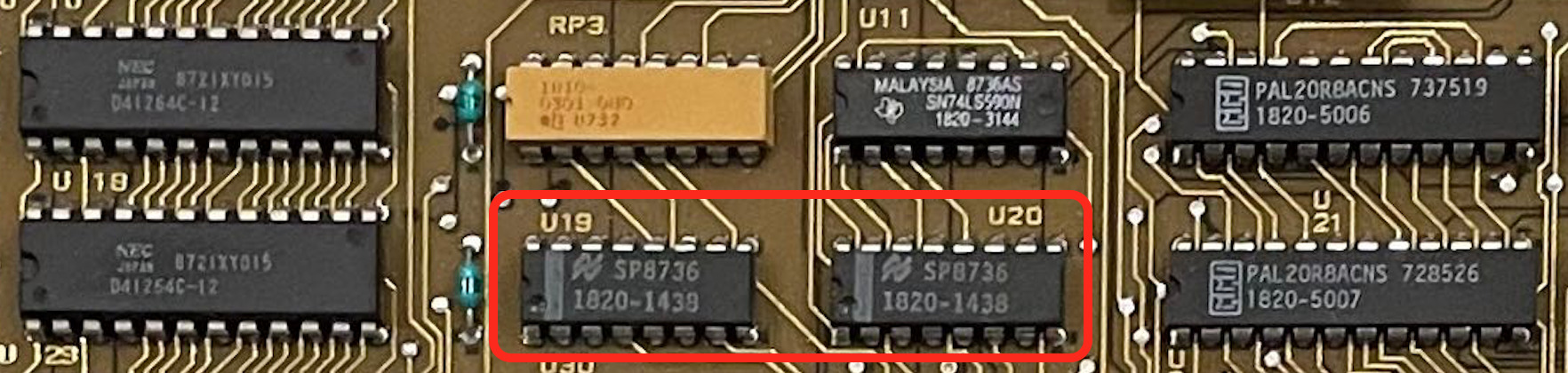
How do you map that to a generic name? By looking up the number in an HP Bench Brief. Bench briefs were a magazine with service information about HP products. In addition to some information about the inner workings of HP equipment, trouble shooting tips, it also contains lists with HP part numbers and their generic name. Like this:

A 1820-1438 corresponds to an SN74LS257, a 4x MUX with tri-state.
You can find the HP Bench Briefs at the Hewlett Packard Archive.
- the National Stock Number or NSN. These are number assigned by the department of defense for inventory handling of replacement parts. You won’t find these numbers on the ICs themselves, but when you’re googling unknown components, you’ll very often run into these.
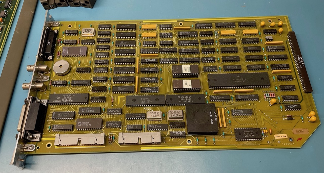
Main Controller Board Overview
The service manual has a good block diagram of the main controller board:
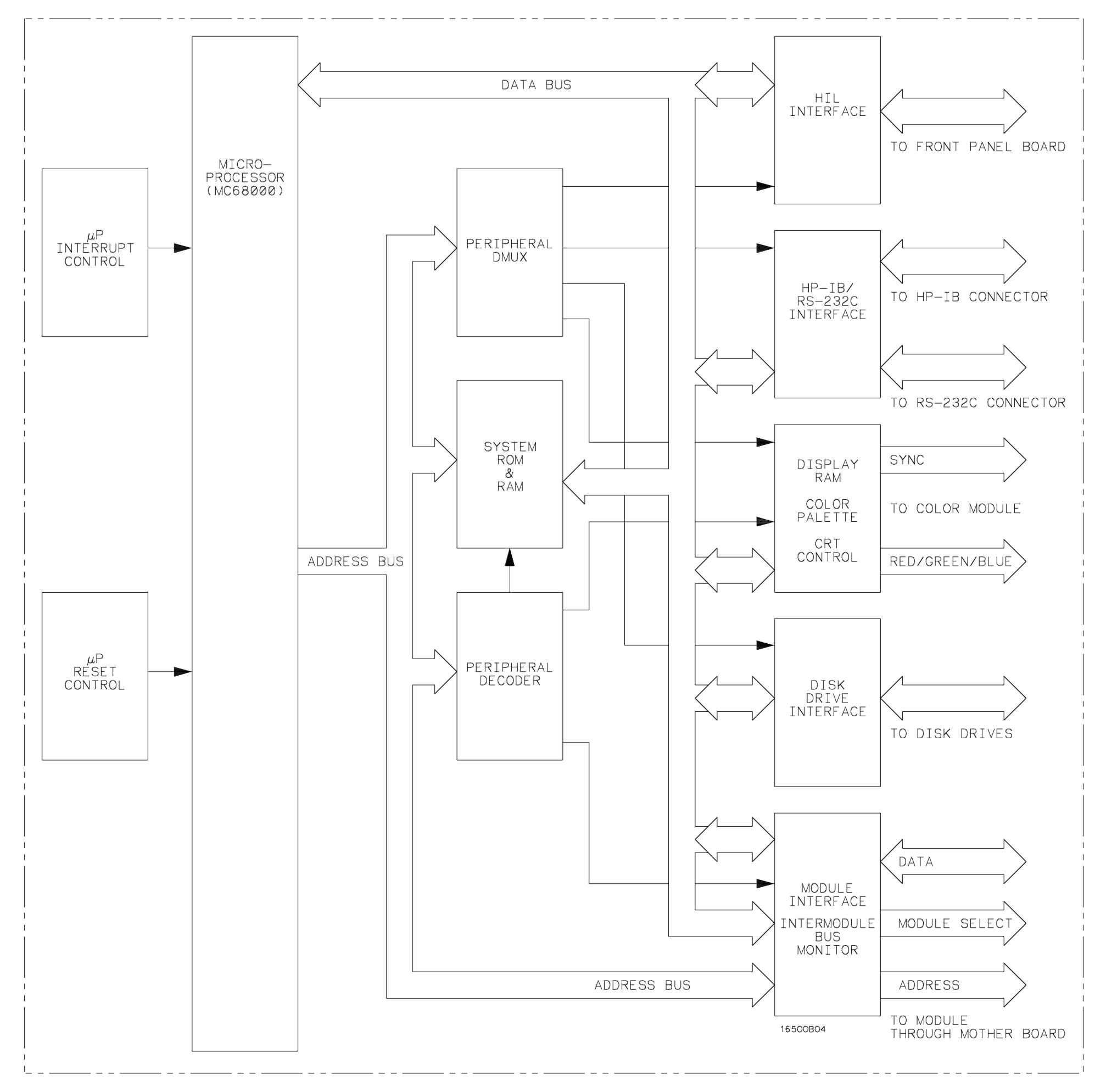 (Click for full size version)
The system is conventional but I still wanted to get a better idea about what exactly made the logic analyzer tick. So I started annotating a few components… and didn’t know where to stop.
The result is the PCB board with all components identified:
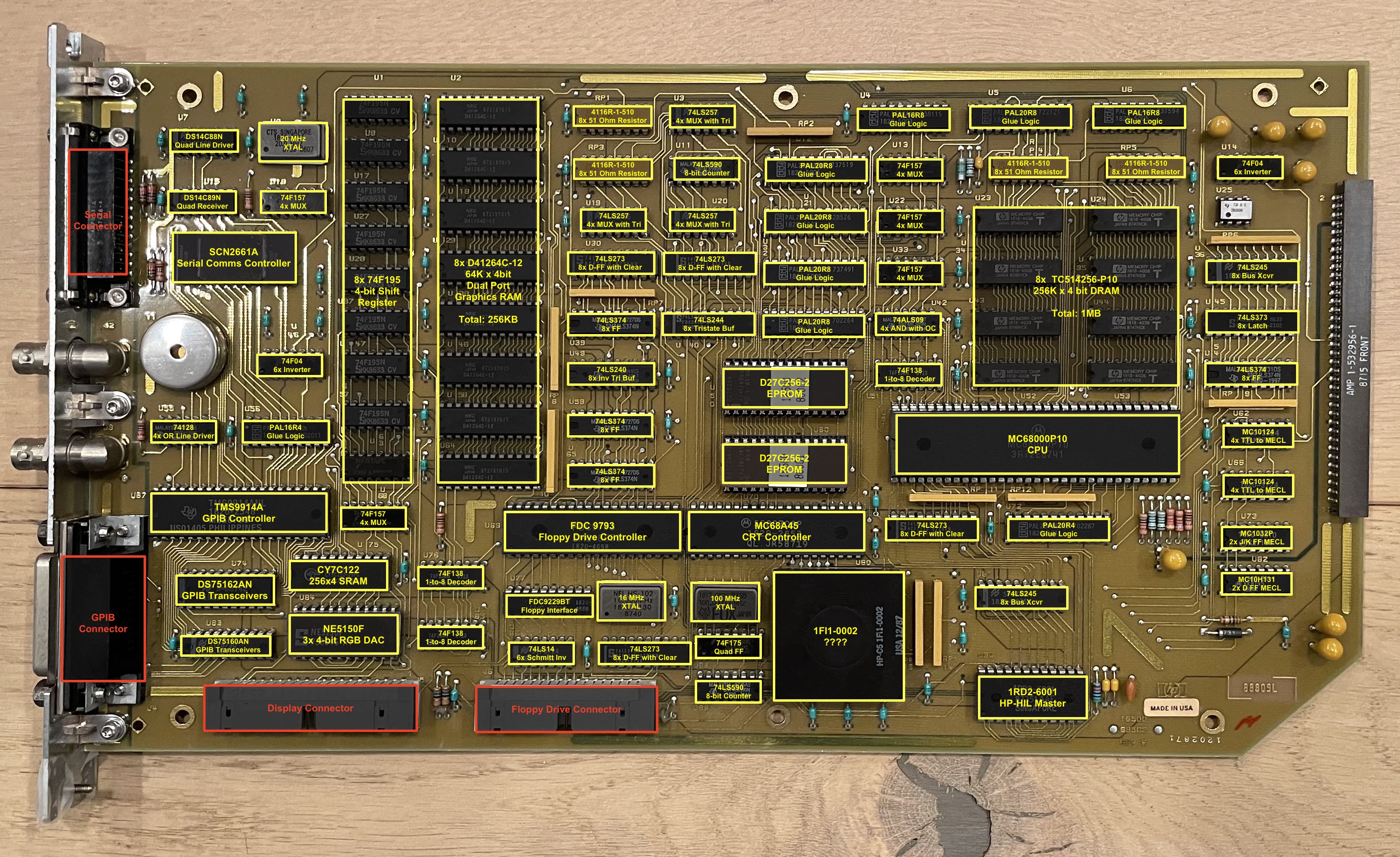 (Click for full size version)
The only major unknown is IC 1FI1-0002 at the bottom. Based on its location and, by elimination, on the block diagram, it’s almost certainly a part of the “Module Interface / Intermodule Bus Monitor”.
CPU System Components
The core of the system consists of the CPU, RAM, and ROM:
-
a good old Motorola 68000 as main CPU
The P10 version is rated at 10 MHz. (User’s Manual)
-
a whopping 1 MByte of DRAM
Built out of 8 256K x 4 bit Toshiba TC514256P-10 ICs.
The -10 version has a row access cycle time of 100ns and the fast page mode cycle time of 55ns, though given the 10MHz clock of the CPU, I doubt that it will do accesses faster than 100ns.
-
32K x 16 bits EPROM
Built with 2 32K x 8 bits D27C256, it contains the initial boot code.
They are the type of EPROM that can be erased by shining a strong UV light through a glass window for 15 to 20 minutes.
I bought a TL866-II EPROM reader on AliExpress to dump the contents of the EPROMs for analysis and reverse engineering in Ghidra. The reader worked great, but soon after doing that somebody pointed out that bitsavers.org already had an archive with the binary images. They also have the service and system reference manuals.
Display Hardware Architecture
The logic analyzer has a CRT with a native resolution of 576x368 pixels. I’ll dive into the details of this CRT in a later blog post, but it’s interesting to see what was driving such a luxurious high resolution display in the early eighties.
-
256 KByte of dual-ported graphics DRAM
576x368 = 212K pixels, so it looks like there’s 1 byte reserved for each pixel.
Built out of 8 instances of 64K x 4 bit NEC D41264C-12 ICs, the DRAMs are grouped as 4 banks of 32K bytes per bank.
These dual-ported DRAMs make it much easier to design a frame buffer without needing to worry about interference between the display scanout logic and the CPU.
As can be seen in the block diagram, the top half has a parallel, random access interface that’s pretty much identical to regular, single ported DRAM. The bottom part contains a shift register that has the size of a single DRAM row. A full row is copied into this register, and then shifted out nibble by nibble.
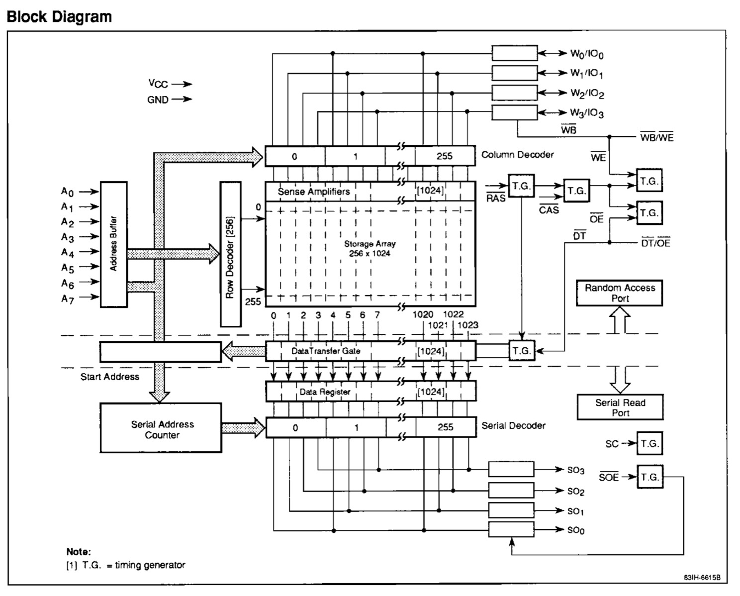
Dual-ported DRAM chips were a thing until sometime in the nineties, but has since completely disappeared: they are signficantly more expensive, and the need for them has gone. With increasing clock speeds, the bandwidth needed to read out pixels from the frame buffer became an ever smaller part of the overall bandwidth, and the logic needed to arbitrate multiple agents was pulled into controller ICs.
-
8 4-bit parallel shift registers
74F195N 4-bit parallel-access shift registers capture the graphics DRAM output.
These are part of a two-stage shift register architecture: the first stage are the shift registers inside the graphics DRAM. Since there are 8 of those in parallel, their outputs get in turn captured in this shift register and then shifted out “downwards” towards the RGB DAC.
-
3x 4-bit video DAC with 16 color palette
The NE5150F takes in a 4 address bits to look up the RGB data of one of 16 colors. Each color is 12 bits, 4 bits per color component. These RGB values are sent to 3 analog DACs.
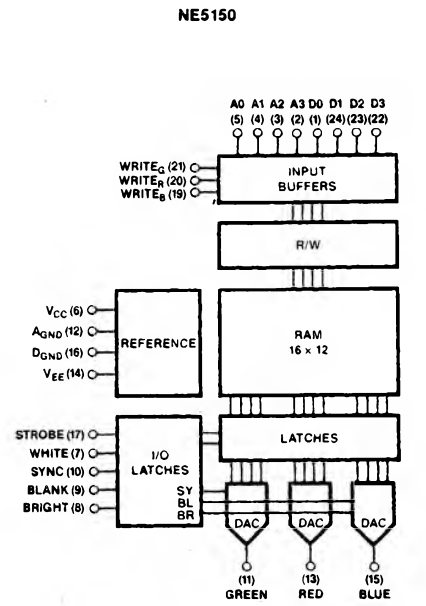
You’d think that these 4 address bits are connected straight to a nibble from parallel shift register, but that doesn’t seem to be the case. Because there’s an additional SRAM that sits in between…
-
256 x 4 bits SRAM
This RAM, a CY7C122-25PC, is a bit of a mystery: the DAC has a palette with 16 entries, good for 16 discrete RGB colors. And yet, this RAM seems to be sitting in between the parallel shift register and the DAC.
Believe it or not, there is a HP 16500A MAME emulator, which confirms that theory: it has a 256-entry
m_palettevariable that takes in an 8-bit value from the graphics RAM to construct the output screen image.So what we have here is double lookup table:
DAC_palette[SRAM_palette[graphics_RAM[address]]].I have no idea why… It certainly doesn’t increase the number of colors (the DAC only support 16), but it’s possible that there are some clever tricks that allow software to distinguish between graphics and text? I stared for quite some time at the disassembled EPROM code and the code that deals with the display controller has a lot of registers operations that deal with masking bits etc.
-
CRT controller
An MC68A45 is the final piece of the display logic. While the previous chips were all part of the graphics data pipeline, this IC contains the main display control logic: video memory address generation and video timing generation for signals such as vsync and hsync.
The 6845 can also generate addresses for a character ROM (for those cases when you don’t use a bitmapped video memory), but I don’t think that functionality is being used by the 16500A: there’s no character ROM on the board, and the EPROM code contains a character set in bitmap format.
Communication Devices
-
GPIB Controller
A TMS9914A is used as GPIB Controller.
It implements the GPIB protocol statemachine and thus relieves the CPU from having to take care of the lower level GPIB logic details.
It does not convert 5V TTL to the analog signalling requirements of the GPIB specification. For that, the HP16500A uses standard DS75160A and DS75162A transceivers. (I’ve been trying to get those for months now on Mouser, but they’re perenially out of stock…)
-
Serial port controller
An SCN2661A handles UART communication. RS-232 voltage level conversion is done by a DS14C88N driver and a DS14C89N receiver.
-
Floppy drive controller
Floppy drive control is handled by two chips: a FDC9793 Floppy Disk Controller/Formatter and a FDC9229BT Floppy Disk Interface Circuit.
HP Human Interface Link Host Controller
Finally, there’s the HP-HIL interface. HIL standards for Human Interface Link, an HP proprietary serial communications protocol that allows connecting multiple external devices to one interface port by daisy chaining them together.
HIL was used for all HP devices that, today, we’d call USB Human Interface Devices: keyboard, mouse, buttons, touch screen, and so forth.
On the 16500A, the embedded touch screen counts as a one HIL device. Further devices such as the keyboard can be plugged in the jack that’s on the front panel.
HP created a number of ASICs for host and devices. The IC that is marked 1RD2-6001 is obviously a host controller. The June 1987 edition of HP Journal has a block diagram of such a host controller:
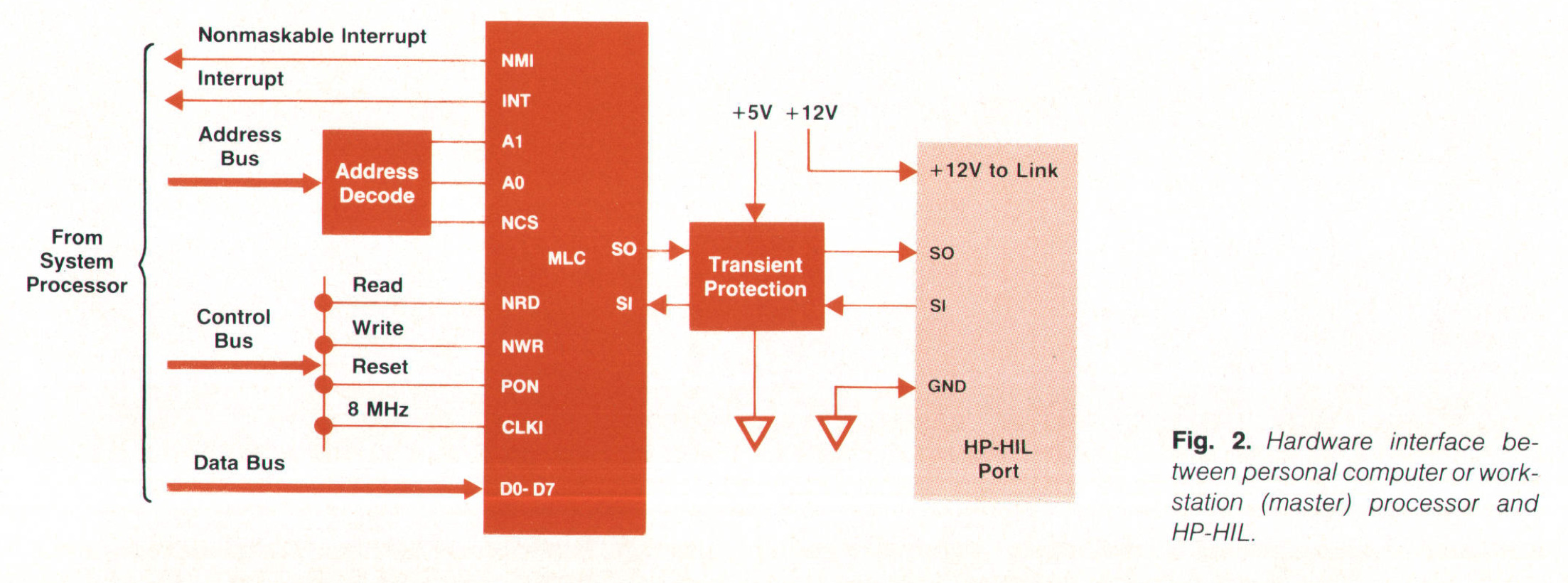
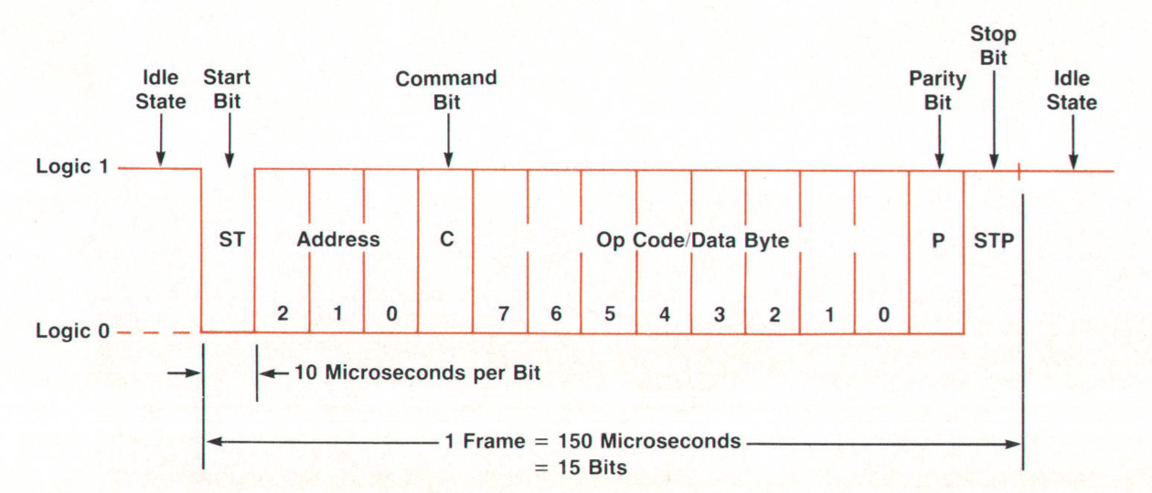
The HIL architecture is quite similar to the way one can daisy-chain multiple SPI devices, with 1 serial data signal going out of the host and one serial data signal returning. The data rate is 100kHz. Unlike SPI, there is no transmit clock, but like a UART, the bit rate is low enough to extract bits with even a low accuracy local clock.
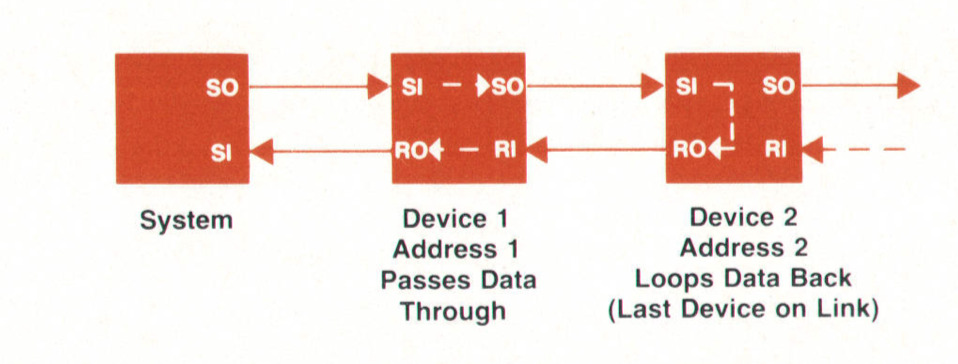
Data is transmitted in frames of 15 bits: 3 address bits, 8 data bits, and start, stop, parity, and command bits. With these 3 address bits, there can be a maximum of 8 devices connected to a single HIL port.
The HP-HIL Technical Reference Manual explains not only the details of the protocol, but also the interface of the HP HIL ASICs.
More Coming Up…
I’ve been playing around with the touchscreen, and that deserves its own write up. The CRT is also a component that has received closer attention: I’ve already done some experiments, and some more are still being worked on.
There’s also a half-baked plan to replace the code of the boot EPROM with code of my own? Maybe run a clone of PacMan on the 68000?
Maybe I’ll even try to use logic analyzer for its original goal: observing signals under test?
So stay tuned for future installments!
References
- HP 16500A/16501A Service Manual
- HP 16500A MAME model
- How to identify integrated circuit (IC) functions from their Hewlett Packard (HP) number
HP HIL
- HIL bus on Wikipedia
- HP-HIL Technical Reference Manual
-
The Hewlett-Packard Human Interface Link
Contains detailed protocol information. Talks about the Master Link Controller (MLC) on the main device, and Slave Link Controller (SLC) on the individual input devices.
-
Implements a HIL to PS/2 keyboard bridge
-
tmk_keyboard project on GitHub
Miscellaneous HIL information