The Intel JTAG Primitive - Using JTAG without Virtual JTAG
- Introduction
- Intel’s JTAG Controller Primitive
- A Huge Caveat when Using the JTAG Controller Primitive
- The JTAG Controller Primitive to Bypass Design Security Features
- Using the JTAG Controller Primitive to Attach Your Own Custom User Scan Chain
- Adding USER0 and USER1 Scan Chains
- A Tracking JTAG TAP FSM to Create a Capture-DR Signal
- An Example Design Tested with OpenOCD
- Conclusion
Introduction
In my blog post about the Intel JTAG UART, I mentioned Intel’s Virtual JTAG system: an ingenious way to connect up to 254 clients to a central JTAG hub, with client discovery features and other good stuff.
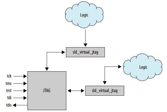
Intel uses it for its own JTAG debug units, JTAG UART, SignalTap, Nios2 debugger, but you can also add your own units.
All of that is is great, but there’s one problem: if you don’t want to use the Quartus SystemConsole (and the pleasure of using $#!#$ Tcl to control it), then you need a bit of a software layer to do JTAG client discovery, select the right JTAG client, and the custom ways to send instructions and data to the client unit.
OpenOCD has this software layer, but it’s only supported for OpenRisc CPUs and its JTAG UART. In an ideal world, OpenOCD should expand that support for many more CPUs and targets, and there was some chatter about it by an Intel employee on the OpenOCD mailing list, but so far it hasn’t happened.
On Xilinx and most Lattice FPGAs, there are easier ways to connect a user-defined JTAG scan chain to the FPGA TAP controller: you just instantiate a BSCANE (Xilinx) or a JTAGG (Lattice) primitive cell, connect one or two chains, and that’s it.
But Intel doesn’t have such a primitive cell… Or so I thought, until somebody mentioned the existence of such a thing in a thread on the /r/FPGA subreddit:
Alternatively you can instantiate the JTAG primitive and bypass the SLD junk. That works fine with OpenOCD. You can see a migen/LiteX example here: https://gist.github.com/jevinskie/811a4fd6deba7fff7280f6908ae37437
The example given is written in Migen, which is amazing if you can stand the syntax (I can’t, unfortunately, and for hobby stuff, I don’t want to use things that I don’t like), but it doesn’t really explain what’s going on.
In this blog post, I show what the primitive does and create my own example in Verilog.
Intel’s JTAG Controller Primitive
So, Intel has a JTAG primitive that can be used to connect your own scan chain. Or better: primitives, because different FPGA families have primitives with a different name:
component arriaii_jtag
component arriaiigz_jtag
component arriav_jtag
component arriavgz_jtag
component cyclone_jtag
component cyclone10lp_jtag
component cycloneii_jtag
component cycloneiii_jtag
component cycloneiiils_jtag
component cycloneiv_jtag
component cycloneive_jtag
component cyclonev_jtag
component fiftyfivenm_jtag
component maxii_jtag
component maxv_jtag
component stratix_jtag
component stratixgx_jtag
component stratixii_jtag
component stratixiigx_jtag
component stratixiii_jtag
component stratixiv_jtag
component stratixv_jtag
component twentynm_jtagblock
component twentynm_jtag
component twentynm_hps_interface_jtag
component fiftyfivenm_jtag
Other FPGA vendors have different primitives as well, Lattice, for example, has JTAGA to JTAGG.
My FPGA board of choice is an Arrow DECA
with a MAX10 FPGA. There’s no max10_jtag primitive in the list above, but fear not, it uses the
fiftyfivenm_jtag block because MAX10 uses a 55nm silicon process.
The ports of the fiftyfivenm_jtag primitive can be found in the fiftyfivenm_atoms.v simulation
library of your Quartus installation, in the ./intelFPGA_lite/20.1/quartus/eda/sim_lib/
directory.
...

module    fiftyfivenm_jtag    (
    tms,
    tck,
    tdi,
    tdoutap,    //controller by fsac_allow_fiftyfivenm_tdoutap INI
    tdouser,
    tmscore,    //controller by sgn_enable_fiftyfivenm_jtag_core_access INI
    tckcore,    //controller by sgn_enable_fiftyfivenm_jtag_core_access INI
    tdicore,    //controller by sgn_enable_fiftyfivenm_jtag_core_access INI
    corectl,    //controller by sgn_enable_fiftyfivenm_jtag_core_access INI
    ntdopinena, //controller by sgn_enable_fiftyfivenm_jtag_core_access INI
    tdo,
    tmsutap,
    tckutap,
    tdiutap,
    shiftuser,
    clkdruser,
    updateuser,
    runidleuser,
    usr1user,
    tdocore             //controller by sgn_enable_fiftyfivenm_jtag_core_access INI
);

    parameter    lpm_type    =    "fiftyfivenm_jtag";

    input tms;
    input tck;
    input tdi;
    input tdoutap;
    input tdouser;
    input tmscore;
    input tckcore;
    input tdicore;
    input corectl;
    input ntdopinena;

    output tdo;
    output tmsutap;
    output tckutap;
    output tdiutap;
    output shiftuser;
    output clkdruser;
    output updateuser;
    output runidleuser;
    output usr1user;
    output tdocore;

...
There’s almost no official documentation for the JTAG primitives, and what does exist is in the context of FPGA design security features. I found Intel application note AN 556: Using the Design Security Features in Intel FPGAs the most useful. Only a small part of the app note talks about the JTAG primitive, but page 32 has the following diagram:
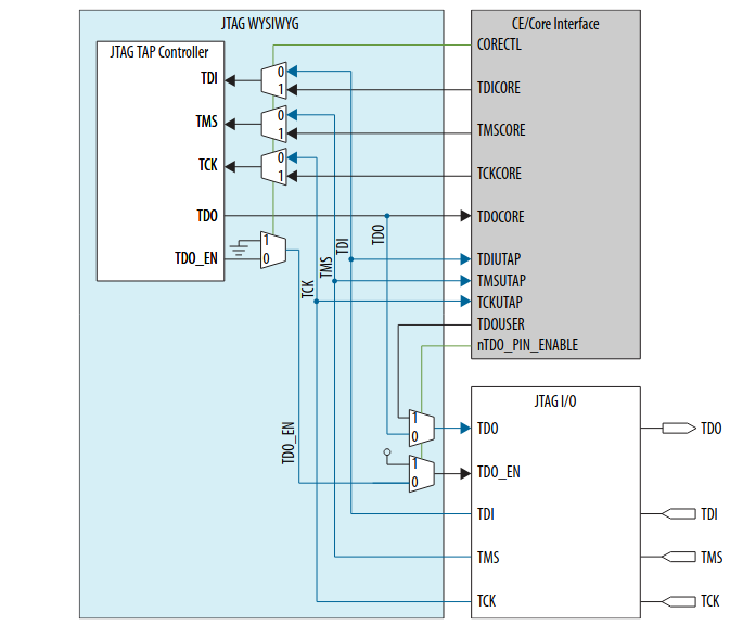
We can see 3 functional regions:
- The section in blue is the primitive itself. It contains a standard JTAG test access port (TAP) controller and some multiplexers. This section is a fixed part of the FPGA, not something that lives in the programmable core region. That makes sense: you need this to load a new bitstream in an empty FPGA.
- The bottom right are the FPGA IO pins that are reserved for JTAG operation. These are the pins to which you connect a USB Blaster if your FPGA board doesn’t have a USB Blaster integrated on the PCB. (The Arrow DECA board has a USB Blaster on the board.)
- The top right lives in the programmable part of the FPGA. This is the part that we can play with.
Don’t take this diagram as gospel: it’s a fairly accurate representation, but some things don’t apply
to the JTAG primitives of all FPGA families. For example, the ntdopinenable pin of the fiftyfivenm_jtag
cell has no impact on my MAX10 design.
A Huge Caveat when Using the JTAG Controller Primitive
You need to be aware of a major issue when you want to bypass the Virtual JTAG infrastructure and roll your own JTAG logic: you can’t use anything anymore that relies on virtual JTAG!
Forget about debugging your design with a SignalTap: it’s not going to happen.
It’s already not common to use JTAG for your own projects, but this restriction makes using the JTAG primitive a hard sell. Still, there are some cases where it might be useful:
- The SLD hub of the virtual JTAG infrastructure requires around 150 logic cells. That’s nothing for a large FPGA, but on something like a MAX10 10M02 with just 2000 logic elements, those 150 cells could be a dealbreaker. (See this post on Intel’s support forum.)
- Designs that were ported over from smaller CPLDs might rely on the JTAG primitive. It’s good to be backward compatible.
- The already mentioned software layer that’s needed to operate virtual JTAG might stand in the way. A good example is my favorite little CPU, the VexRiscv. Its JTAG debug unit along with its custom version of OpenOCD (see my earlier blog post) can be made to work with pretty much any JTAG chain, but virtual JTAG is not supported.
- The JTAG primitive makes it possible to open up certain design security features that were locked down with a fuse. This is not important for hobby designs, but there are production situations where this can be important.
The JTAG Controller Primitive to Bypass Design Security Features
The official documentation talks about the JTAG primitive in the context of FPGA design security features. Most hobbyists will not use those, but it’s still interesting in its own right, so let’s look at this first.
The most important usage of an FPGA JTAG port is to load a bitstream into the FPGA or to program a bitstream into a connected flash PROM. But modern FPGAs have all kinds of additional production and deployment related features that are controlled by JTAG:
- programming a non-volatile bitstream decryption key (one time only!)
- loading a volatile bitstream decryption key
- programming a tamper protection fuse
- checking the tamper protection status
- JTAG access lock
- …
For each of these features, there’s a corresponding JTAG instruction.
On Intel FPGAs, the JTAG access lock feature is particularly interesting: it disables all non-standard JTAG instructions.
Only IEEE specification mandatory JTAG instructions such as BYPASS, IDCODE, EXTEST are enabled in the JTAG TAP controller.
All others, both non-mandatory IEEE instruction as well as Intel custom instructions, are disabled.
(See table 17 of the AN 556 application note.)
JTAG access lock is automatically enabled for FPGAs that have the tamper protection fuse blown.
However, there may be cases where you want to reenable the advanced JTAG features. For example to enable a debug feature on a working product after entering some secret unlock procedure.
It is possible to disable the JTAG access lock by shifting the UNLOCK instruction into the JTAG controller… but how can you do that when all non-standard instructions were disabled?!
Intel has the perfect solution for that: the JTAG primitive has the corectl pin, an option to drive the FPGA TAP controller
with internal signals instead of the external JTAG IOs. So if you want to disable access lock, your own design needs
to create a JTAG-compatible trace.
The application note describes how to use the JTAG primitive in that kind of situation. It even provides a design example.
Using the JTAG Controller Primitive to Attach Your Own Custom User Scan Chain
With the access security part behind us, let’s look at the more interesting, undocumented, part: attaching you own custom scan chain to the JTAG TAP.
The Intel JTAG primitive pins can be divided in different categories:
Standard JTAG TAP Control Pins
The first 4 pins are the standard JTAG pins. They must be connected directly to the FPGA JTAG IO pins.
| Signal Name | Direction | Description |
|---|---|---|
tck |
input | FPGA TCK IO pin |
tms |
input | FPGA TMS IO pin |
tdi |
input | FPGA TDI IO pin |
tdo |
output | FPGA TDO IO pin |
In Quartus, the JTAG IO pins have the altera_reserved_ prefix. All you need to
do is wire them up like this:
module top(
        input  wire     clk,
        input  wire     button,
        output reg      led0,
        output reg      led1,
        output reg      led2,

        input  wire     altera_reserved_tck,
        input  wire     altera_reserved_tms,
        input  wire     altera_reserved_tdi,
        output wire     altera_reserved_tdo
    );

...

    fiftyfivenm_jtag u_jtag(
        .tms(altera_reserved_tms),
        .tck(altera_reserved_tck),
        .tdi(altera_reserved_tdi),
        .tdo(altera_reserved_tdo),

...
When the JTAG primitive is present in a design, Quartus will automatically assign the altera_reserved_ JTAG pins
to the right IO pads.
Alternate Core JTAG TAP Control Signals
The next signals are the alternate JTAG signals that are used to control the JTAG TAP from the FPGA core logic. These are the pins that are used in the earlier described access unlock situation when you want the core logic to send JTAG commands to the TAP.
| Signal Name | Direction | Description |
|---|---|---|
corectl |
input | Switch JTAG TAP pins to alternate control pins. 0: TAP is controlled by external IO pins. 1: TAP is controlled by FPGA core logic. |
tckcore |
input | Alternate TCK pin that comes from the core logic |
tmscore |
input | Same as TCK but for TMS |
tdicore |
input | Same as TCK but for TDI |
tdocore |
output | Alternate TDI pin that comes to the core logic |
For our use case, we can simply strap corectl to 0 to always control the
JTAG TAP with external IOs.
Some Intel FPGAs, such as the Cyclone 10 LP family, don’t support tckcore,
tmscore, tdicore and corectl pins. You could just not wire them up
and count on Quartus strapping them to 0 by default…
IMPORTANT: Don’t assign a value of 1 to corectl and then flash such a design into your FPGA unless you REALLY
know what you’re doing. Doing so disconnects the FPGA TAP controller from the JTAG IO pins and makes it
impossible to reflash the FPGA!!!
User JTAG Signals
| Signal Name | Direction | Description |
|---|---|---|
tckutap |
output | TCK signals that currently being used by the FPGA TAP controller. |
tmsutap |
output | Same as TCK but for TMS. |
tdiutap |
output | Same as TCK but for TDI. |
tdoutap |
input | Exists on some, but not all, Intel FPGA primitives. Don’t connect. |
The 3 output signals are intended to be used by the FPGA core logic when it needs the signals that are being used by the TAP controller.
When corectl is set to 0, these 3 signals will carry the same value as the
external FPGA IO pins tck, tms, tdi pins. You could just use the IO pins,
but it’s cleaner to use the ...utap signals.
You can use these signals if you want to create your own JTAG TAP FSM that tracks the internal state of the FPGA JTAG controller, or to shift data in one of your own USER shift registers. See below.
User Scan Chain Control Signals
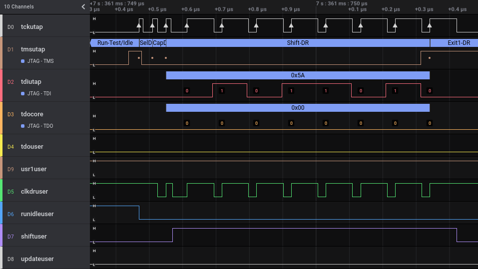
The next signals are some of the most useful ones if you want to quickly connect your own scan chain to the FPGA TAP controller.
I could not find any official documentation for any of these signals, but it was easy to figure out after bringing them out to some FPGA GPIOs and recording transactions with a Saleae Logic Pro 16 logic analyzer.
The Intel JTAG TAP controller supports tons of proprietary instructions, usually not documented, that are used
for all kinds of production and releated features. But it also has the USER0 and USER1 instructions (with
IR codes 0x00c and 0x00e resp.) that exist to create 2 user defined scan chains in the FPGA core logic.
The virtual JTAG infrastructure normally makes heavy use of these, but when not using that, we can use them as we want.
| Signal Name | Direction | Description |
|---|---|---|
usr1user |
output | High when the IR register is set to USER1. |
clkdruser |
output | TCK clock when when IR is USER0 or USER1 and the TAP states are Capture-DR or Shift-DR. |
shiftuser |
output | High when IR is set to USER0 or USER1 and the TAP state is Shift-DR. |
updateuser |
output | High when IR is set to USER0 or USER1 and the TAP state is Update-DR. |
runidleuser |
output | High when IR is set to USER0 or USER1 and the TAP state is Run-Test/Idle. |
tdouser |
input | Routed to TDO when IR is set to USER0 or USER1. |
The signals above are sufficient to implement basic user scan chain functionality.
Adding USER0 and USER1 Scan Chains
We now have enough signals to shift new values in user0 and user1 scan chains, and copy them over into user0 and user1 register:
    reg [7:0] user0_shiftreg = 0;
    reg [7:0] user0_reg      = 0;

    reg [7:0] user1_shiftreg = 0;
    reg [7:0] user1_reg      = 0;

    always @(posedge tckutap) begin
        if (!usr1user) begin
            if (shiftuser)
                user0_shiftreg  <= { tdiutap, user0_shiftreg[7:1] };

            if (updateuser)
                user0_reg       <= user0_shiftreg;
        end
        else begin
            if (shiftuser)
                user1_shiftreg  <= { tdiutap, user1_shiftreg[7:1] };

            if (updateuser)
                user1_reg       <= user1_shiftreg;
        end
    end

    always @(negedge tckutap) begin
        tdouser  <= !usr1user ? user0_shiftreg[0] : user1_shiftreg[0];
    end
The code is trivial, but there’s one problem: while we can shift in new values, and copy the value of the shift register into the value register, there is no way to capture an internal value into the shift register right before shifting the value out of the chip.
For some inexplicable reason, Intel supplies a shiftuser and an updateuser signal,
but no captureuser signal?!
A Tracking JTAG TAP FSM to Create a Capture-DR Signal
Capturing a value right before a shift operation is a very common way to extract data out of a chip through JTAG.
The lack of a captureuser signal can be remedied by adding an FSM in the core logic that tracks the states of the
FPGA TAP. We can do this by using the tckutap and tmsutap signals.

There are million open source JTAG TAP FSM implementations out there. I’d be remiss if I didn’t add one myself:
    localparam jtag_exit2_dr            = 0;
    localparam jtag_exit1_dr            = 1;
    localparam jtag_shift_dr            = 2;
    localparam jtag_pause_dr            = 3;
    localparam jtag_select_ir_scan      = 4;
    localparam jtag_update_dr           = 5;
    localparam jtag_capture_dr          = 6;
    localparam jtag_select_dr_scan      = 7;
    localparam jtag_exit2_ir            = 8;
    localparam jtag_exit1_ir            = 9;
    localparam jtag_shift_ir            = 10;
    localparam jtag_pause_ir            = 11;
    localparam jtag_run_test_idle       = 12;
    localparam jtag_update_ir           = 13;
    localparam jtag_capture_ir          = 14;
    localparam jtag_test_logic_reset    = 15;

    reg [3:0] jtag_fsm_state = 15;

    always @(posedge tckutap) begin
        case(jtag_fsm_state)
            jtag_test_logic_reset: jtag_fsm_state <= tmsutap ? jtag_test_logic_reset : jtag_run_test_idle;
            jtag_run_test_idle   : jtag_fsm_state <= tmsutap ? jtag_select_dr_scan   : jtag_run_test_idle;
            jtag_select_dr_scan  : jtag_fsm_state <= tmsutap ? jtag_select_ir_scan   : jtag_capture_dr;
            jtag_capture_dr      : jtag_fsm_state <= tmsutap ? jtag_exit1_dr         : jtag_shift_dr;
            jtag_shift_dr        : jtag_fsm_state <= tmsutap ? jtag_exit1_dr         : jtag_shift_dr;
            jtag_exit1_dr        : jtag_fsm_state <= tmsutap ? jtag_update_dr        : jtag_pause_dr;
            jtag_pause_dr        : jtag_fsm_state <= tmsutap ? jtag_exit2_dr         : jtag_pause_dr;
            jtag_exit2_dr        : jtag_fsm_state <= tmsutap ? jtag_update_dr        : jtag_shift_dr;
            jtag_update_dr       : jtag_fsm_state <= tmsutap ? jtag_select_dr_scan   : jtag_run_test_idle;
            jtag_select_ir_scan  : jtag_fsm_state <= tmsutap ? jtag_test_logic_reset : jtag_capture_ir;
            jtag_capture_ir      : jtag_fsm_state <= tmsutap ? jtag_exit1_ir         : jtag_shift_ir;
            jtag_shift_ir        : jtag_fsm_state <= tmsutap ? jtag_exit1_ir         : jtag_shift_ir;
            jtag_exit1_ir        : jtag_fsm_state <= tmsutap ? jtag_update_ir        : jtag_pause_ir;
            jtag_pause_ir        : jtag_fsm_state <= tmsutap ? jtag_exit2_ir         : jtag_pause_dr;
            jtag_exit2_ir        : jtag_fsm_state <= tmsutap ? jtag_update_ir        : jtag_shift_ir;
            jtag_update_ir       : jtag_fsm_state <= tmsutap ? jtag_select_dr_scan   : jtag_run_test_idle;
        endcase
    end

    wire capture_dr;
    assign capture_dr    = (jtag_fsm_state == jtag_capture_dr);
capture_dr will go high whenever the FSM passes throught the Capture-DR state. In combination with the
usr1user signal, we can use this to capture a new value into the USER1 shift register, but we can’t do
that for USER0 because there’s no separate usr0user signal. If we want that, we need to track the contents
of the IR register as well:
    // The Intel IR register is 10-bits
    reg [9:0] ir_shiftreg = 0;
    reg [9:0] ir_reg = 0;

    always @(posedge tckutap) begin
        if (jtag_fsm_state == jtag_shift_ir) begin
            ir_shiftreg <= { tdiutap, ir_shiftreg[9:1] };
        end

        if (jtag_fsm_state == jtag_update_ir) begin
            ir_reg <= ir_shiftreg;
        end
    end
We can now create a captureuser signal, and use that to capture a value in the USER0 shift register before
shifting out.
The example below increments a counter whenever the USER0 scan chain sees a capture-DR event, and shifts out the value of that counter:
    wire captureuser;
    assign captureuser = capture_dr && (ir_reg == 10'h00c || ir_reg == 10'h00e);

    reg [7:0] user0_shiftreg = 0;
    reg [7:0] user0_reg      = 0;

    reg [7:0] user0_counter  = 0;

    always @(posedge tckutap) begin
        if (!usr1user) begin
            if (captureuser) begin
                user0_shiftreg  <= user0_counter;       // <----
                user0_counter   <= user0_counter + 1;   // <----
            end

            if (shiftuser)
                user0_shiftreg  <= { tdiutap, user0_shiftreg[7:1] };

            if (updateuser)
                user0_reg       <= user0_shiftreg;
        end
        else begin
            if (shiftuser)
                user1_shiftreg  <= { tdiutap, user1_shiftreg[7:1] };

            if (updateuser)
                user1_reg       <= user1_shiftreg;
        end
    end

    always @(negedge tckutap) begin
        tdouser  <= !usr1user ? user0_shiftreg[0] : user1_shiftreg[0];
    end
An Example Design Tested with OpenOCD
You can find a working example in my intel_jtag_primitive_blog repo on GitHub.
It contains the pieces of code above merged together and with a few more lines to:
- capture the value of a button in bit 0 of the USER1 register
- drive 3 LEDs with the value of bits [2:0] of the USER1 register
USER0 is only used to count the number of times that it has been acccessed (as shown in the code above.)
The code has been tested on my Arrow DECA board, but it should be trivial to adapt it to any board with an Intel FPGA.
You can test it as follows:
- Compile the code with Quartus
- Load the bitstream into the FPGA
-
In one terminal window, start OpenOCD:
/opt/openocd/bin/openocd \
  -f interface/altera-usb-blaster2.cfg  \
  -c "jtag newtap max10 fpga_tap -expected-id 0x031050dd -irlen 10"
This command first connects to a USB-Blaster2, which is the kind of USB Blaster that’s on the DECA board.
It then declares that this board is expected to have a JTAG TAP controller with a 10-bit instruction register, all Intel FPGAs have that, and an IDCODE of 0x031050dd, a 10M50 MAX10 FPGA.
After running the command above, you should see something like this:
Open On-Chip Debugger 0.10.0+dev-01236-gc974c1b7-dirty (2021-07-17-21:18) Licensed under GNU GPL v2 For bug reports, read http://openocd.org/doc/doxygen/bugs.html Info : only one transport option; autoselect 'jtag' Info : Listening on port 6666 for tcl connections Info : Listening on port 4444 for telnet connections Info : Altera USB-Blaster II found (Firm. rev. = 1.39) Info : This adapter doesn't support configurable speed Info : JTAG tap: max10.fpga_tap tap/device found: 0x031050dd (mfg: 0x06e (Altera), part: 0x3105, ver: 0x0) Warn : gdb services need one or more targets defined -
In a different terminal window, you can now telnet into the OpenOCD session:
telnet localhost 4444Trying 127.0.0.1... Connected to localhost. Escape character is '^]'. Open On-Chip Debugger >You can select the USER0 scan chain like this:
irscan max10.fpga_tap 0x00cDo a bunch of scan operation on the USER0 chain:
> drscan max10.fpga_tap 8 0xff
00
> drscan max10.fpga_tap 8 0xff
01
> drscan max10.fpga_tap 8 0xff
02
> drscan max10.fpga_tap 8 0xff
03
> drscan max10.fpga_tap 8 0xff
04
The value of 0xff that gets shifted into the USER0 chain gets ignored, but you can see an incrementing value being shifted out, as expected.
Similarly, you can select the USER1 scan chain like this:
irscan max10.fpga_tap 0x00eIn the example below, scanning values of 0x01, 0x02, and 0x00 result in different LEDs being switched on and off. The output values of 0x01 and 0x00 depend on whether or not you press one of the buttons at the time of issuing the
drscancommand.> irscan max10.fpga_tap 0x00e > drscan max10.fpga_tap 8 0x01 01 > drscan max10.fpga_tap 8 0x02 01 > drscan max10.fpga_tap 8 0x00 00 > drscan max10.fpga_tap 8 0x00 00
Conclusion
JTAG is a bit of an obscure topic, and even more so for hobby electronics. But there are cases where it can be useful: attaching a debugger to an embedded CPU is the most common one. The Intel virtual JTAG system is a little bit heavy, but the only one that’s well documented.
In this blog post, I tried to document a way to use that native JTAG port while bypassing the virtual JTAG system, and provide a working example design.
There are quite a bit of negatives in using this technique, but maybe, one day, you’ll have a need for it. When that day comes, I hope that the information provided here will be helpful.