The Intel JTAG UART - Add a Serial Console to Your Design without Extra IO Pins
- Introduction
- What’s a JTAG UART?
- An Open Source JTAG UART?
- The Intel’s Virtual JTAG System
- The Intel JTAG UART
- Adding a JTAG UART to Your Design without Using Platform Designer
- Connecting to the JTAG UART with nios2-terminal
- Communicating to the JTAG UART with a Script
- References
Introduction
In my previous blog post about updating the RAM initialization contents of Intel FPGAs, I mentioned how I include a small CPU in almost all my designs for things like low-speed interface control, register initialization, overall data flow management etc.
Another essential item in my design toolbox is the JTAG UART.
Everybody is probably familiar with the regular UART, a serial interface that dates back to somewhere in the seventies that is present in systems everywhere, from the lowest performance embedded microcontrollers to high level routers and servers, where it’s used as a console interface to enter commands or to dump logging messages.
It’s a simple protocol that’s easy to implement on FPGA with just a handful of combinational logic and flip-flops.
And yet I almost never use it.
That’s because, for all its simplicity, it still requires an extra cable from my FPGA board to my host PC, and at least 2 pins of the FPGA. If UARTs were the only way to quickly implement a console in my designs, I would use it, but there’s an alternative: the JTAG UART.
The JTAG UART offers the benefits of a UART without the downside of requiring an additional cable: it uses the JTAG connection that is already there to load new bitstreams into the FPGA or to program the FPGA configuration flash.
JTAG UARTs can be added to all FPGAs that have a JTAG test access port (TAG), but they are especially easy to use on Intel FPGAs. And since those are the FPGAs that I use for the development of all my projects, that’s what this blog post will be about.
What’s a JTAG UART?
To the embedded soft CPU inside the FPGA, a JTAG UART behaves just the same as a regular UART: a block with a handful of control and status registers to write bytes to a transmit FIFO, read bytes from a receive FIFO, and to check if there those FIFOs are full or empty.
But on the other side, instead of a piece of logic that serializes the data to and from some external IO pins, it’s connected to a JTAG TAP of the FPGA.

On the PC, there’s the usual low level driver to control the JTAG dongle, and some higher level software that sends out the right JTAG commands set control bits, check status bits, and transfer data.
Advantages over a regular UART
- No extra cable between FPGA board and PC required.
- Doesn’t require additional functional IO pins.
- Multiple JTAG UARTs per FPGA possible, e.g. one per CPU core, all over the same JTAG connection.
- Potentially higher data transfer speeds, depending on the JTAG clock.
Disadvantages
-
No JTAG UART standard.
Xilinx and Intel have a JTAG UART, but their implementations are very different and incompatible with each other.
-
There is no JTAG UART protocol specification.
Because the low-level JTAG instructions to interact to the JTAG UARTs aren’t published, you can’t write your own driver to talk the JTAG UART on your Xilinx or Intel FPGA.
And thus…
-
Requires closed source tools to control.
Intel and Xilinx provide tools to talk to the JTAG UART. I’m only familiar with the Intel tools, and the interactive terminal tool works well enough, but it’s an incredible pain to interact with the JTAG UART by script.
For almost all my designs, I only use the JTAG UART to type some commands and get debug information, without a need to script things. For that, the Intel tools are totally sufficient.
An Open Source JTAG UART?
If JTAG UART is so great, why isn’t there are open source alternative?
It turns out that there is! It’s called “JTAG Serial Port” in the OpenRisc OR1K world. It even has mainline support in OpenOCD, with support for the Intel Virtual JTAG TAP, the Xilinx BSCAN TAP, and the so-called “Mohor” TAP (I think it’s a generic JTAG TAP that’s implemented by Igor Mohor).
However, there’s very little information about it, and while there must be RTL for this block somewhere, I wasn’t able to find it.
The availibility of an officially software driver in OpenOCD is a big deal though, so if somebody wants to plug this hole in the open source FPGA ecosystem: go for it!
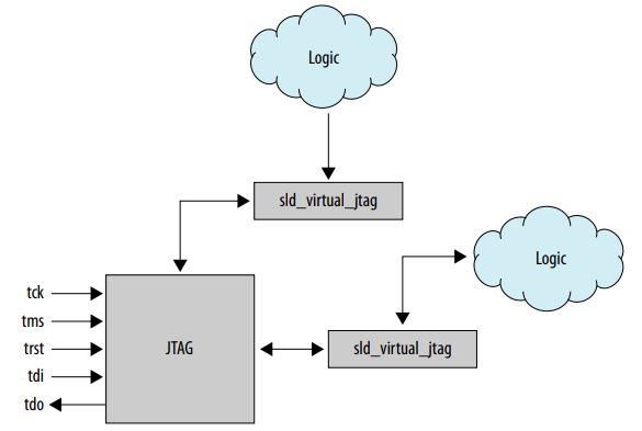
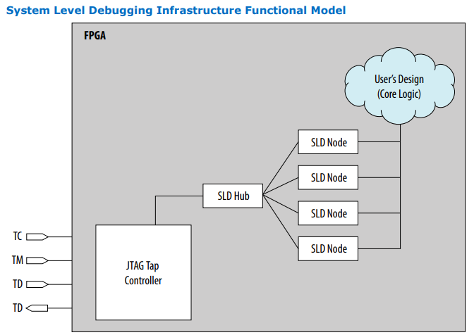
The Intel’s Virtual JTAG System
Xilinx and some Lattice FPGAs have a way to link to the native JTAG TAP by instantiating a particular JTAG primitive cell, but there’s no general framework to add any random amount of JTAG clients.
Intel’s solution is completely different: it offers Virtual JTAG, a system where up to 254 JTAG related clients can be attached to the native JTAG TAP. Each JTAG client has its own instruction register and data registers.
All of this is part of Intel’s System Level Debug (SLD) infrastructure. (When you’re compiling
a design with Quartus, you might see modules being compiled that start with sld_. Chances
are that this is related to virtual JTAG.)
The virtual JTAG system has a central hub that offers discoverability features: you don’t need to know up front and specify what kind of JTAG clients are in the FPGA design, the Intel tools will figure that out by themselves by enumerating the clients that are connected to the hub.
Here are some examples of Intel’s own clients:
- JTAG UART
- SignalTap
- In-System Sources and Probes
- Nios2 CPU debugger
A user can also design their own custom clients. When added to an Intel FPGA, the earlier mentioned OpenRisc JTAG Serial Port would be such a client.
It’s out of the scope of this blog post to dive into the low level details. If you’re interested, you can read up on it in Intel’s Virtual JTAG User Guide.
The Intel JTAG UART
The Intel JTAG UART is not complicated.
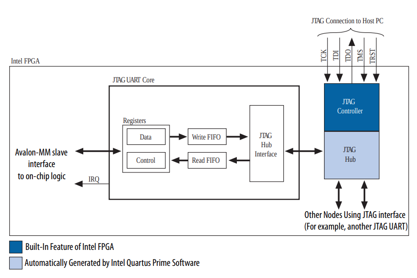
On one side, it links to the virtual JTAG hub. There’s a transmit and receive FIFO to buffer up traffic bursts.
On the user logic side, it has an Intel Avalon bus with access to 2 registers, data and control:
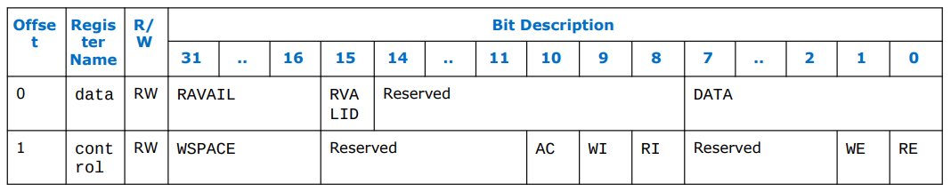
See the Intel documentation for the details.
Adding a JTAG UART to Your Design without Using Platform Designer
The most common way to add a JTAG UART to your design is adding one to a Nios2 SOC system in Intel’s Platform Designer (formerly known as Qsys.) In that case, it’s as simple as drag-and-drop, and the RTL, the software driver and everything else get autogenerated for you.
But that’s not what I will show here: it’s one thing to tie your debug logic to a proprietary feature, it’s another to make your whole design depend on a proprietary CPU architecture and tool flow. I develop my designs on Intel FPGAs because of the excellent debug features, but I still want to be able to run the final, debugged, result on a Lattice FPGA! You can’t do that with a Nios2-based system.
Instead, I’ll extend the VexRiscv-based mini CPU design of my previous blog post with a JTAG UART.
A full project that runs on an Arrow DECA FPGA
can be found in this jtag_uart_example repo on GitHub.
Intel FPGA have had support for a JTAG UART for years. Porting the design to a different FPGA such as the Cyclone II based EP2C5T144 development board is trivial. And when it’s time to run the design on a different brand FPGA, I just comment out this:
`define JTAG_UART
Step 1: Create a JTAG UART primitive
Ok, I lied. If you’re not copying the code from my example design, you’ll need to use
Platform Designer once to create a jtag_uart module that you can instantiate
in your design.
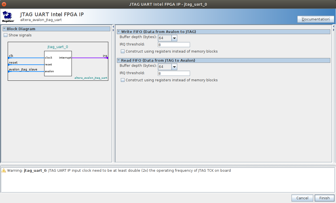
Create a system with just a JTAG UART:
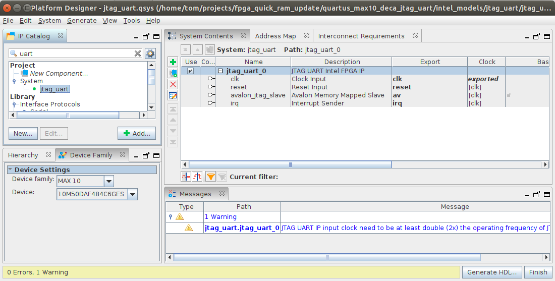
The number of parameters to choose from is limited to just some TX and RX related FIFO settings:
Save the Qsys file and generate all the logic in its own jtag_uart directory
underneath an intel_models directory. All these files
are added to the GitHub repo. I can reuse them from one project to the next without ever launching Platform
Designer again, even if I change to a different Intel FPGA type.
Step 2: Add the JTAG UART to your design
The jtag_uart_bb.v
file has all the ports of the jtag_uart module:
module jtag_uart (
	av_chipselect,
	av_address,
	av_read_n,
	av_readdata,
	av_write_n,
	av_writedata,
	av_waitrequest,
	clk_clk,
	irq_irq,
	reset_reset_n);

	input		av_chipselect;
	input		av_address;
	input		av_read_n;
	output	[31:0]	av_readdata;
	input		av_write_n;
	input	[31:0]	av_writedata;
	output		av_waitrequest;
	input		clk_clk;
	output		irq_irq;
	input		reset_reset_n;
endmodule
There’s a clock and reset, an Intel Avalon bus that needs to be wired up to the CPU bus, and an interrupt if you care about that. (I generally don’t.)
What’s striking is what is not there: some JTAG related signals. When you sythesize the design, Quartus internally wires up the module to the virtual JTAG infrastructure. This doesn’t get exposed in your own code.
The Avalon bus behavior is similar to an ARM APB bus, and straightforward to wire up as long as you’re prepared to deal with wait cycles.
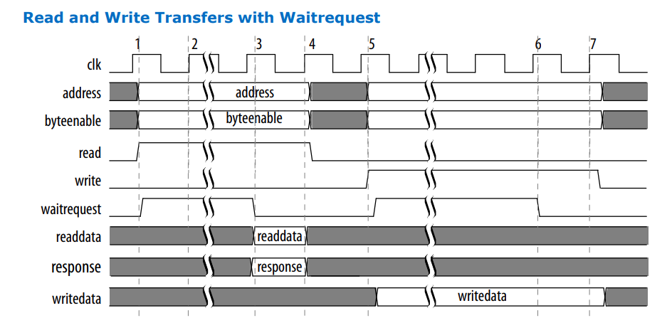
The diagram above shows read and write signals, while the JTAG UART module has read_n and write_n. That’s
because the creators of the Avalon Interface Specification
couldn’t make up their mind and decided to support both variants.
If you’re using SpinalHDL, the code to make it work with a real APB bus would look something like this:
    av_chipselect    := io.apb.PENABLE && io.apb.PSEL.orR
    av_address       := io.apb.PADDR(2)
    av_write_n       := !io.apb.PWRITE
    av_read_n        := io.apb.PWRITE
    av_writedata     := io.apb.PWDATA

    io.apb.PRDATA       := av_readdata
    io.apb.PREADY       := !av_waitrequest
But in my example Verilog design, I’m connecting it to the split command/response dBus of the VexRiscv:
    assign jtag_uart_sel        =  dBus_cmd_valid && (dBus_cmd_payload_address[31:28] == 4'h9);

    assign jtag_uart_cs         = jtag_uart_sel;
    assign jtag_uart_addr       = dBus_cmd_payload_address[2];
    assign jtag_uart_read       = !dBus_cmd_payload_wr;
    assign jtag_uart_write      = dBus_cmd_payload_wr;
    assign jtag_uart_wdata      = dBus_cmd_payload_data;

    // cmd is acknowledged when the waitrequest is dropped...
    assign jtag_uart_dBus_cmd_ready = !jtag_uart_waitrequest;

    // ... and the response is returned the cycle after acknowledging cmd.
    always @(posedge clk) begin
        jtag_uart_rd_done <= 1'b0;
        if (jtag_uart_cs && jtag_uart_read && !jtag_uart_waitrequest) begin
            jtag_uart_rdata     <= jtag_uart_readdata;
            jtag_uart_rd_done   <= 1'b1;
        end
    end

	jtag_uart u_jtag_uart (
		.clk_clk        (clk),
		.reset_reset_n  (!reset),
		.av_chipselect  (jtag_uart_cs),
		.av_waitrequest (jtag_uart_waitrequest),
		.av_address     (jtag_uart_addr),
		.av_read_n      (!jtag_uart_read),
		.av_readdata    (jtag_uart_readdata),
		.av_write_n     (!jtag_uart_write),
		.av_writedata   (jtag_uart_wdata),
		.irq_irq        ()
	);
Step 3: Create a tiny software driver
Instead of using Intel’s software driver, I’ll be talking to the hardware directly through my own tiny driver:
The core API is just 3 function calls:
void jtag_uart_tx_char(const char c);
void jtag_uart_tx_str(const char *str);
int  jtag_uart_rx_get_char(uint8_t *c);
You’ll probably want to extend this with a custom printf function, but this is good enough for this
example.
Step 4: Add JTAG UART support to your firmware
The rest is up to your imagination.
I extended my LED toggling example by adding an r command that reverses the order in which
the LEDs are toggled.
When a different character is pressed, a help message is printed out instead.
void help()
{
    jtag_uart_tx_str(
            "r:     reverse LED toggle sequence\n"
            "\n"
        );
}

int main()
{
    jtag_uart_tx_str("Hello World!\n");

    int reverse_dir = 0;

    while(1){
        int wait_time = REG_RD_FIELD(STATUS, BUTTON) ? 200 : 100;

        unsigned char c;
        if (jtag_uart_rx_get_char(&c) != 0){
            jtag_uart_tx_str("Command: ");
            jtag_uart_tx_char(c);
            jtag_uart_tx_char('\n');

            if (c == 'r'){
                jtag_uart_tx_str("Reversing LED sequence...\n");
                reverse_dir ^= 1;
            }
            else{
                help();
            }
        }

        if (reverse_dir){
            REG_WR(LED_CONFIG, 0x04);
            wait_led_cycle(wait_time);

            REG_WR(LED_CONFIG, 0x02);
            wait_led_cycle(wait_time);

            REG_WR(LED_CONFIG, 0x01);
            wait_led_cycle(wait_time);
        }
        else{
            REG_WR(LED_CONFIG, 0x01);
            wait_led_cycle(wait_time);

            REG_WR(LED_CONFIG, 0x02);
            wait_led_cycle(wait_time);

            REG_WR(LED_CONFIG, 0x04);
            wait_led_cycle(wait_time);
        }
    }
}
Step 5: Add a testbench simulation stub
I need a skeleton version of the JTAG UART to make sure that the testbench compiles without error, and can run the CPU code without hanging.
    always @(posedge clk_clk) begin
        av_waitrequest      <= 1'b1;
        av_readdata         <= 32'h0001_0000;


        if (av_chipselect && !cs_d) begin
            av_waitrequest  <= 1'b0;
        end


        cs_d    <= av_chipselect;
    end
This code could be much smarter! Right now, all it does is return a “1” at bit 16. This makes the FW of the CPU believe that there’s data available in the write FIFO, so it won’t get into an endless loop polling this field when it wants to write transmit a character.
Connecting to the JTAG UART with nios2-terminal
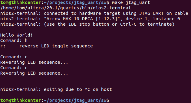
After compiling the software and synthesizing the design to a bitstream, all that remains is loading the bitstream into the FPGA, and connecting to the JTAG UART.
I use nios2-terminal for the last step. It comes with a Quartus installation.
When there’s only 1 JTAG UART in your design, and the Quartus ./bin directory is part of your PATH, just
run:
nios2-terminal
It should response with something like this:
nios2-terminal: connected to hardware target using JTAG UART on cable
nios2-terminal: "Arrow MAX 10 DECA [1-12.3]", device 1, instance 0
nios2-terminal: (Use the IDE stop button or Ctrl-C to terminate)

Hello World!
Command: h
r:     reverse LED toggle sequence

Command: r
Reversing LED sequence...
Command: r
Reversing LED sequence...
Having a console to control your FPGA design can be an enormous productivity boost. At the press of a key, you can reprogram the behavior of your design to test various modes, print out internal status register etc.
If you already have a tiny CPU system as part of the design, the additional cost of adding a JTAG UART is trivial: a handful of flip-flops, 2 RAMs for the FIFOs, and, in this case, 100 bytes of additional code space.
Communicating to the JTAG UART with a Script
Talking to the JTAG UART with a scripting language like Python is so painful that I just avoid it. But for those who needs it, here are some pointers to get your started.
Communication happens through the Quartus System Console. The System Console provides all accesses to the debug resources inside the FPGA through services. The JTAG UART is a Bytestream Service. Check out the manual here.
The System Console uses TCL, the most wretched of all scripting languages ever invented.
- Start the System Console from the main Quartus GUI with [Tools] -> [System Debugging Tools] -> [System Console].
-
Expand the hierarchical tree in the left top window under “devices”.
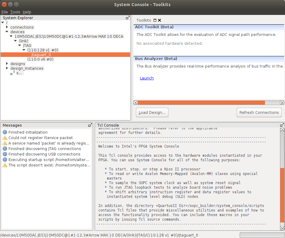
In my design, there are only 2 instances under “JTAG”: the virtual JTAG hub (ID 110:0 v6), and the JTAG UART (ID 110:128 v1). If I had added a SignalTap, or more JTAG UARTs, they would all show up in this list.
-
Enter the following TCL commands in the bottom right command windows:
  set bytestream [lindex [get_service_paths bytestream] 0]
  set claimed_bytestream [claim_service bytestream $bytestream mylib]
  set payload [list 114]
  bytestream_send $claimed_bytestream $payload
This does the following:
-
Get a reference to the JTAG UART.
The ‘0’ refers to the first JTAG UART in the design. In our case, there’s only 1.
-
Claim the JTAG UART for exclusive use.
This command will fail if you already have nios2-terminal running, so make sure you stop that first.
-
Create a list of bytes to send to that JTAG UART.
114 is the ASCII code for ‘r’, the command to reverse the order of the LED toggling sequence in my design.
-
Send the list of bytes to the JTAG UART.
You should see the LEDs sequence swap into the opposite direction.
-
To make things reliable, you’ll have to pull the JTAG UART reply, etc. And to be able to use a non-disgusting scripting language like Python, you’d need some kind of server code bridges the TCL and the Python world.
This is all very doable, but let’s just leave that for another time.