The $37 Arrow DECA FPGA Board
Executive Summary: it’s the new default FPGA board for my hobby projects.
- Introduction
- DECA Board Features
- DECA Board Flaws
- The DECA Design Resources Archive
- In the Box
- Compiling a First Design
- Conclusion
- References
Introduction
For as long as there are people who are interested in trying out FPGAs, there will be questions about which board to start with, preferably for a low price.
There is no one perfect answer to this: there’s a huge variety in FPGA types, board peripherals and features, and prices. Some people are fine with commercial vendor tools, for other, an open source tool flow is essential.
But at the end of January 2021, an unexpected contender entered the market: the $37 Arrow DECA board with a MAX 10 10M50 FPGA. Add $4 sales tax and $6 for USPS shipping and it’s yours for a grand total of $47.
Don’t make the mistake of thinking that this is a new product. On the contrary, this board was introduced in 2015 and all that time, it has been for sale for $169.
The new price is almost certainly an end-of-life firesale, but at the time of writing this, 3 months after the initial excitement of the new price, the Arrow Electronics website still shows 1314 items in stock. That should be sufficient to satisfy a quite a bit of new FPGA hobby entrants and experts alike.
Edit: as of September 16, 2021, the stock is gone.
While working a different work-in-progress blog post, I decided to give the DECA board a try. Here are my impressions…
DECA Board Features
The DECA board is small, but it’s packed with features.
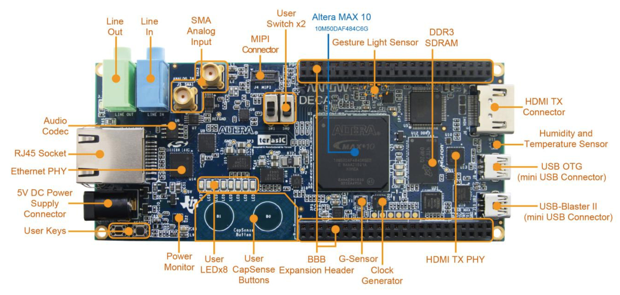
You should check out the user manual for the details, but here are some stand-out items:
-
MAX10 10M50 FPGA
I’ve been using a $200 Intel MAX10 development kit with the same 10M50 FPGA for work related stuff, and I love this FPGA: it has a lot of resources. It has analog inputs. Instead of off-chip serial configuration flash, it has on-chip parallel flash. There’s plenty of block RAM and DSP resources. 4 PLLs for all your clocking needs. And ~50K of logic elements should be enough for everyone!
The biggest drawback is the speed. The main focus of the MAX10 product line are fast bootup times (they’re intended to be used as MAX-II CPLD replacements), and low power consumption, not peak clock speeds.
A Max10 FPGA can run a VexRiscv soft core at ~100MHz, which is a far cry of the 240MHz that’s reported for the already dated and not terribly fast Artix-7.
-
Built-in USB-Blaster II
No need for an external JTAG dongle means no additional cost, a more compact board, faster bitstream downloads, and less awkward cabling on your crowded workbench.
-
A set of periperals that’s sufficient to create your own small computer
- 512MB of DDR3 DRAM
- HDMI output: up to 1080p @60Hz with support for audio as well. (It even has HDCP.)
- USB OTG port: while OTG never really took off, it allows you to use the USB port as a host or as a device.
- 10/100 Ethernet
- MicroSD flash card socket
- 64MB of QSPI flash, fully usable because the bitstream is stored on the FPGA itself.
- Audio line in/line out with 24-bit audio CODEC
In combination with the 50K logic elements of the FPGA, these peripherals are more than sufficient to create a Linux-capable system with display, keyboard, network support, and a flash storage drive.
Or you could port a retro gaming emulator to it.
-
A large variety of additional peripherals
- BeagleBone compatible I/O expansion connectors with digital GPIOs and analog inputs
- the usual assortment of LEDs, buttons, and switches
- humidity and temperature sensor, an accelerometer, capacitive key sensor, an additional temperature sensor (because two is better than one!)
- analog inputs, including 2 with SMA connector and pre-amplifier
- MIPI connector for camera sensors
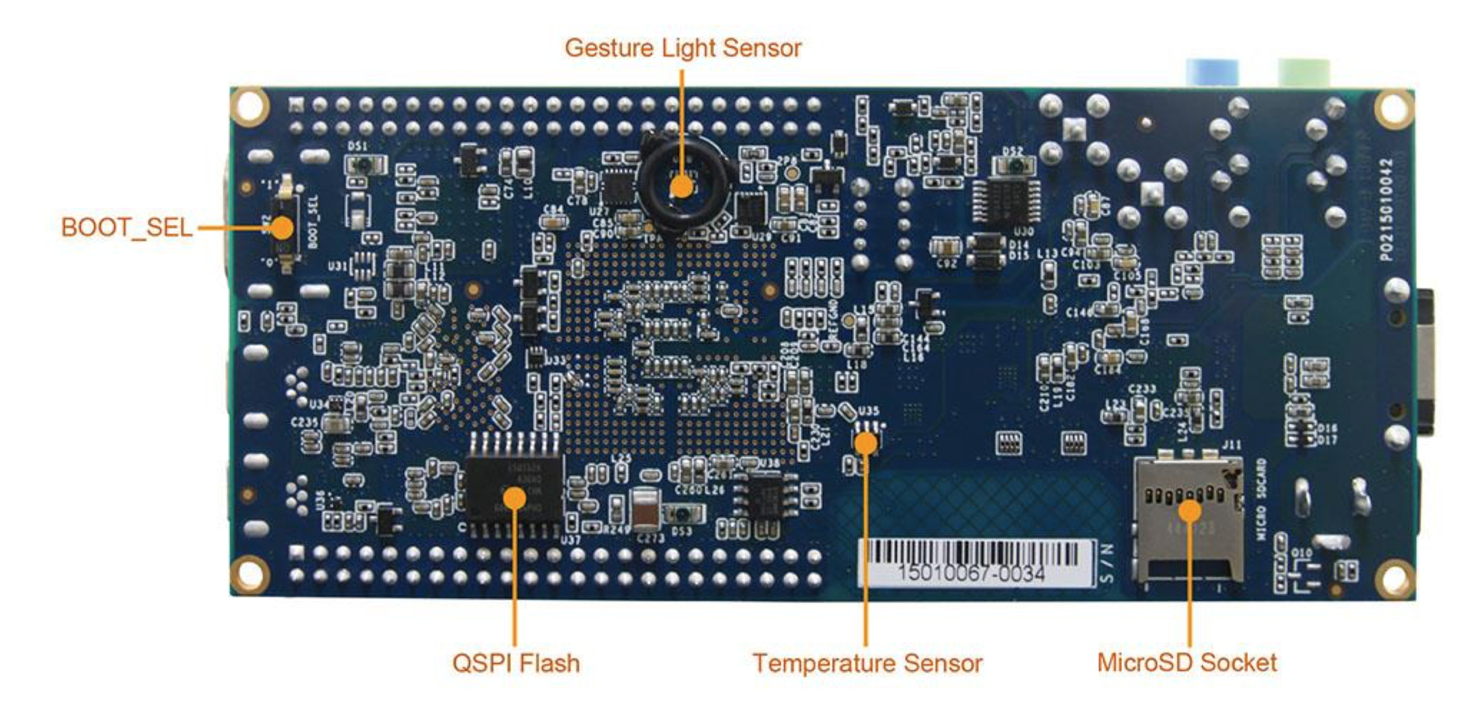
- a dual-boot/dual-config switch
There’s really something for everybody!
The reason for 2 temperature sensors is because one is close to the FPGA to measure the temperature of the electronics, while the humidity/temperature sensor is on the outskirts of the PCB to measure ambient temperature and humidity.
DECA Board Flaws
It’s hard to find major flaws with this board, but here are a few minor ones:
-
End-of-life product means disappearing design resources
The Arrow product website still has working links to the user manual, product brief, schematic and BOM, but the DECA wiki page link is dead, and there’s no trace of the design resources archive that’s supposed to come with it. The cost to host that 150MB file must be simply too high for a world-wide company like Arrow…
I rarely use the example code or example designs that comes with FPGA boards: give me a schematic and part numbers, and I can usually figure out the rest myself. But working with FPGAs is my full-time job. And even then, I ran into some Quartus settings and configuration issue before I was able compile my first bitstream!
For a beginner, the lack of this information can be a deal-breaking road block.
Luckily, that design resources archive is still available for download on the Terasic website, though you need a create an account to access it.
-
Hardly any non-official resources
This was never a very popular product, probably due to its price, so there are hardly any hobbyist projects that use this board.
-
no PMOD connector support
The BeagleBone compatible I/O connectors support 69 digial IOs and 7 analog inputs, but they are not compatible with the very popular PMOD standard, like the 2 in the picture below:
It’s not difficult to rewire some pins to make a PMOD device work, but it won’t be the seamless plug-and-play of other FPGA boards.
I’m thinking of making a small BeagleBone to PMOD adapter PCB.
-
the dual-boot/dual-config BOOT_SEL switch is very fragile
It’s not a big deal since I don’t really care about this functionality, but I broke the switch the first time I toggled it…
-
The SystemBuilder tool that’s part of the design resources is Windows only
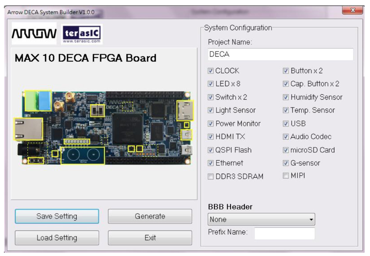
The SystemBuilder is a GUI to create new project configuration files. I personally don’t need it, but it can be a great help in getting some basics right.
The DECA Design Resources Archive
The design resources archive is pretty great and comprehensive.
It contains:
- board schematic
-
user manual
The user manual goes over all major features of the board, describes the power and clock architecture, has tables with IO pin assignment information, shows how to create a new project from scratch with the SystemBuilder (again, Windows only), and goes over all the included example designs.
-
25 demo designs for most (all?) peripherals
Each demo design contains source code, Quartus project files (timing constrains, pin and IO bank voltage assignments, …), digital output files (bitstream, compiled C code if there’s a CPU in the design), and Quartus compilation report files.
The design files were compiled with Quartus 15. Quartus hasn’t seen a lot of changes since then, but there have been updates to the way libraries and handled, so if you have enough disk space, I’d just install that version for a smooth experience.
Some of the demo designs require interaction with a host PC and include an executable. Again, only Windows executables are provided.
- datasheets for all active components of the board
In the Box
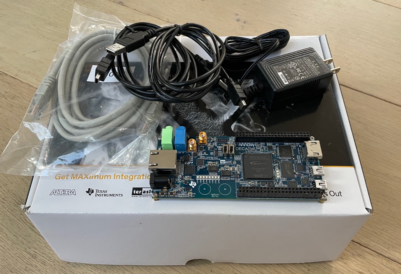
The DECA board itself is quite small. The box it came in was not. In addition to the board itself, it came with a 5V power brick (not needed when the board is connected to USB), a 110V power cable, 2 mini-USB cables, and an Ethernet cable.
Compiling a First Design
When I started using the board, I hadn’t discovered the design resources archive on the Terasic website yet, so I had to figure out some critical Quartus constraints myself.
IO Bank Voltage Rails and IO Pin Configuration Parameters
For those who are not familiar with complex FPGAs: one of the most important things to get right are the voltages of the IO banks. The 10M50 has 9 different IO banks, and each IO bank can be assigned a different IO voltage. The selected voltage must be compatible with the required IO voltage standard of the IO pins.
For example, if a periperal component has a 3.3V I2C interface, and thus requires 3.3V IOs to control the interface, the IO bank in which the IOs are located must be connected to a 3.3V power rail, and the bitstream must be configured accordingly.
The user manual warns that incorrect IO bank and pin assigments may damage the board. It helpfully lists the pin assignment parameters, but it doesn’t bother to include a table with the IO bank voltages.
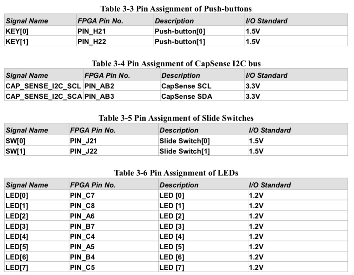
Getting this right is a matter of going through the schematic and copying over the correct values:
set_global_assignment -name IOBANK_VCCIO 2.5V -section_id 1A
set_global_assignment -name IOBANK_VCCIO 2.5V -section_id 1B
set_global_assignment -name IOBANK_VCCIO 2.5V -section_id 2
set_global_assignment -name IOBANK_VCCIO 3.3V -section_id 3
set_global_assignment -name IOBANK_VCCIO 3.3V -section_id 4
set_global_assignment -name IOBANK_VCCIO 1.5V -section_id 5
set_global_assignment -name IOBANK_VCCIO 1.5V -section_id 6
set_global_assignment -name IOBANK_VCCIO 1.8V -section_id 7
set_global_assignment -name IOBANK_VCCIO 1.2V -section_id 8
My trial design with a clock input, a button, and 3 leds has the following pin assignments:
set_instance_assignment -name IO_STANDARD "2.5 V" -to clk
set_instance_assignment -name IO_STANDARD "1.5 V" -to button
set_instance_assignment -name IO_STANDARD "1.2 V" -to led0
set_instance_assignment -name IO_STANDARD "1.2 V" -to led1
set_instance_assignment -name IO_STANDARD "1.2 V" -to led2
The values above can be entered with the Pin Assignment window of Quartus GUI, or you can
paste them in the <project_name>.qsf file. You can also find them
in my demo design.
Device Configuration Options
After assigning the IO bank values, I expected smooth sailing in getting a bitstream to compile, but the Quartus fitter bailed out with an error:
It turns out that the DECA board uses a voltage of 1.2V for IO bank 8, which makes certain default device configuration options impossible.
It took a bit of Google work to find the right settings:
set_global_assignment -name AUTO_RESTART_CONFIGURATION ON
set_global_assignment -name ENABLE_CONFIGURATION_PINS OFF
set_global_assignment -name ENABLE_BOOT_SEL_PIN OFF
After that, my design compiled, and it worked too.
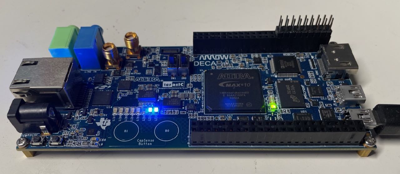
The design can be found here.
It is nothing more than an LED blinky, but that’s always an important pipe cleaner for me.
Conclusion
At $37, the Arrow DECA board is excellent for anyone who wants to play with FPGAs. It has most of the peripherals that I need, and the large FPGA makes it possible to fit all my designs while still allowing plenty of space to include generously sized SignalTap logic analyzers for debugging.
It’s now my standard FPGA board for my hobby projects.