A Pixel Purse LED Cube Controlled by a Cisco 3G Modem
I presented this project at BangBangCon West 2020, but never got around to publish a blog post about it. A 10 minute talk is not enough to cover some technical aspects, and since I’m starting to forget them, it’s about time to write things down.
- Introduction
- PCBs for Mechanical Structures
- Cube Assembly - First Try
- Cube Assembly - Second Try
- HWIC Interface & HUB75 Adapter Boards
- Overall FPGA Digital Design
- Correcting for Panel Orientation and Location in the HUB75 Streamer
- From One to Two HUB75 Ports
- Rick, Pac-Man, Mario
- Unexpected Short Circuits Solved with UV Hardened Glue
- Powering the Cube
- Integrating It All and Shortcuts
- Presenting at !!Con West
- Looking Back…
- References
Introduction
I can’t pinpoint exactly when it happened, but there was a time, between 2018 and 2020, when LED cubes were a bit of thing in the world of hobby electronics.
On Twitter, I followed day-by-day the journey of kbob (aka Bob Miller) as he tried to come up with the best possible 3D printed solution. The end result was amazing.
He also wrote a blog post with a history of LED cubes as well as some implementation details.
At the Hackaday Superconference 2019, Greg Davill took things to the next level After first building something with off-the-shelve LED matrix panels, like kbob and everybody else, he designed one from scratch, LED PCB and aluminum frame included.
I always wanted to do something with LED panels myself, but there wasn’t a catalyst until October 2019, when the Pixel Purse went on sale on Amazon for $6.16. (As I write this, the price is back at $52.)
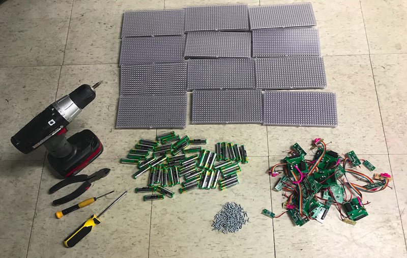
I wrote a Pixel Purse Teardown blog post, but what I didn’t mention back then was that I bought not 1 but 12 purses: just what you need to cover the 6 sides of a cube. This was not as easy as you’d think: Amazon had a limit of only 2 purses per customer, but I recruited 5 victims at work and soon enough this stack of boxes was dropped off at my work cubicle:
![]()
The loot after disassembling all of them:
- 12 32x16 LED panels
- 48 AA batteries (low quality!)
- 12 4Mbit SPI flash PROMs
- a bunch of screws and voltage regulators
Even with the most important components in hand, I didn’t actually started building anything: my attention had shifted to other projects. But at the end of November, Josh asked me if I had anything interesting to present for the upcoming !!Con West 2020?
I did not, but I wondered if I could make an LED cube by using my reverse engineered Cisco HWIC-3G-CMDA modem as LED panel driver?
On December 22nd, 2019, I received confirmation that my “Cisco Purses Cubed!” talk proposal had been accepted, and “please, confirm your participation by December 30th.” At that point, I had nothing but the LED panels and the Cisco modem. There was no RTL code, no way to connect the modem to the LED HUB75 interface, and no plan for the mechanical structure.
But there was the Christmas holiday!
Over the course of a couple of days, I was able to get 2 panels to light up in a way that wasn’t totally random, which made me confident enough to foolishly confirm at the last moment that yes, I’d be able to present my cube at the end of February. Meanwhile, my wife had picked up some rumors about a virus on Chinese forums and was wondering whether she should cancel an upcoming business trip to Wuhan.
The race was on!
PCBs for Mechanical Structures
PCB are an example of high precision manufacturing at mass scale yet low cost. And we, hobbyists, can go along for the ride for next to nothing: a company like JLCPCB will deliver 5 quality PCBs for $2 + $5 shipping if you can wait 3 weeks. Add another $9, and the time from initial order to PCBs at your doorstep can be 6 days!
I had just received a Thanksgiving sale 3D printer, but with only 2 months left to go, there was no time to learn 3D modelling and how to use the printer from scratch. A laser cutter was out for the same reason, so I decided on using PCBs for the mechanical structure that would keep the LED panels together.
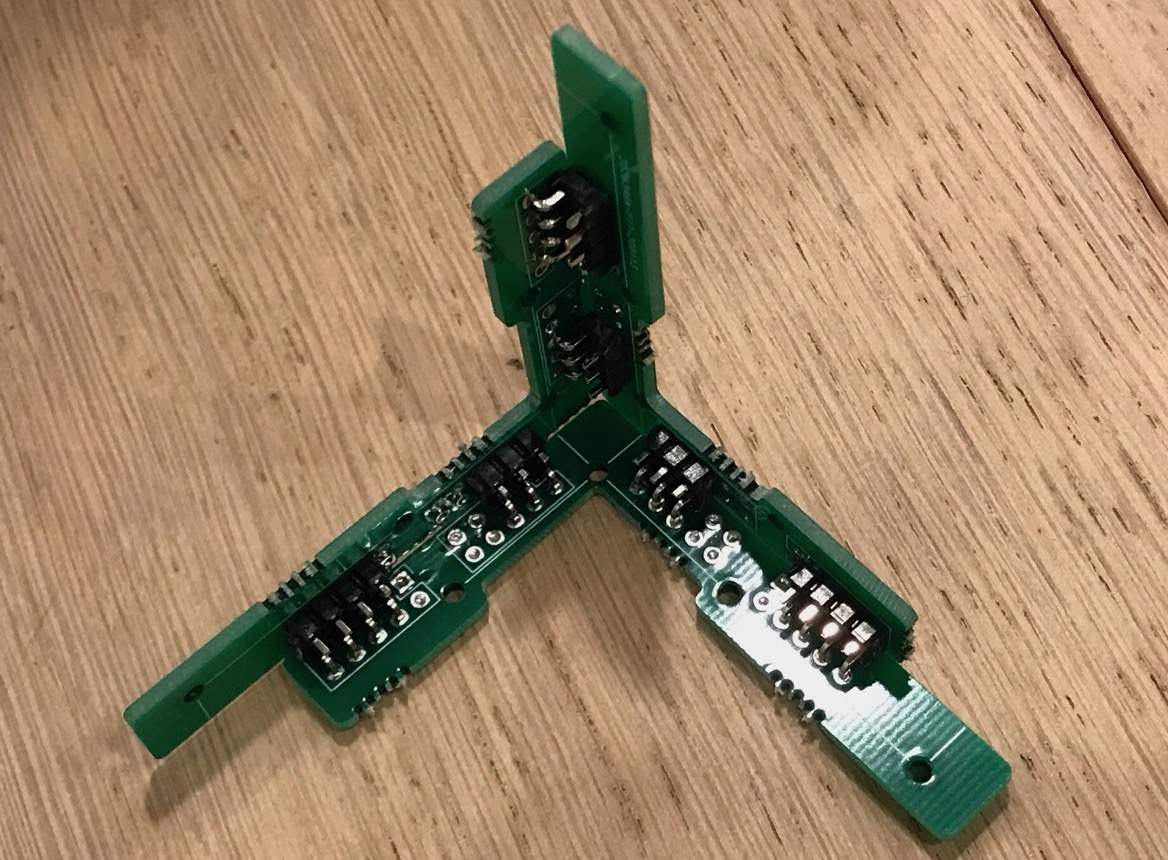
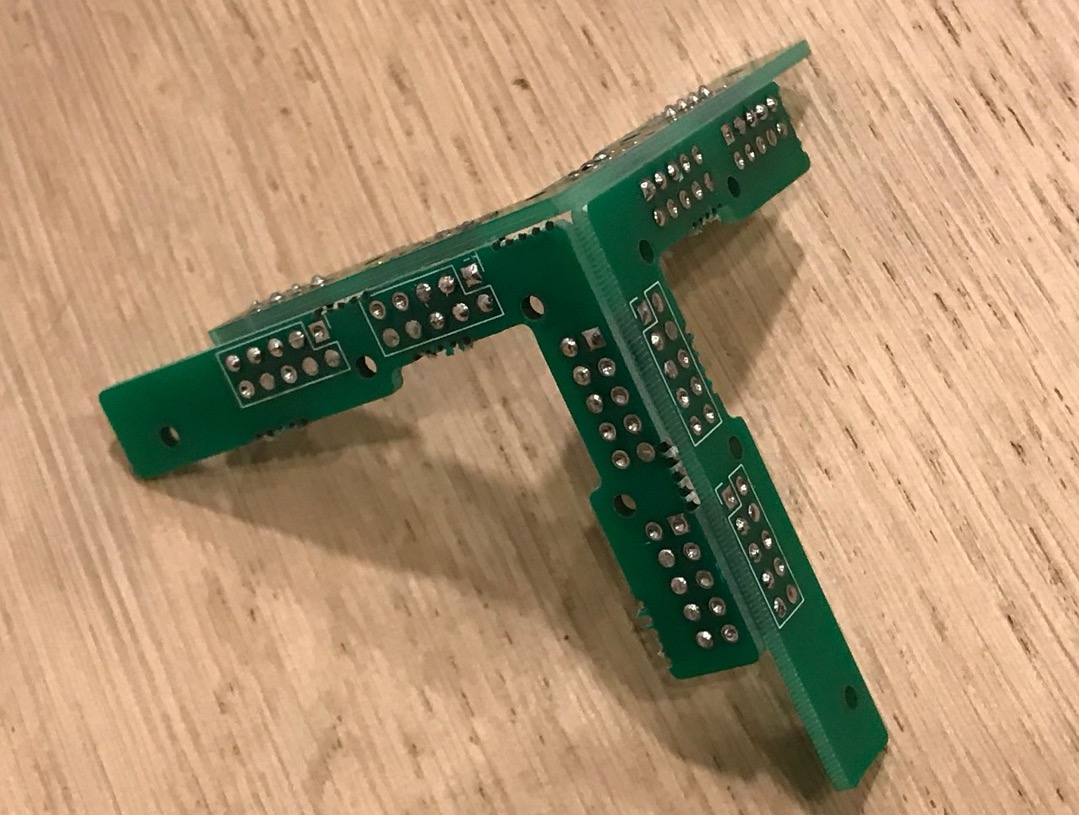
The idea was to build 8 corner pieces that each consist of 3 identical corner brackets, and to solder 90 degree pin headers to fuse the 3 brackets into a solid unit.
Each of the 24 brackets looked like this:
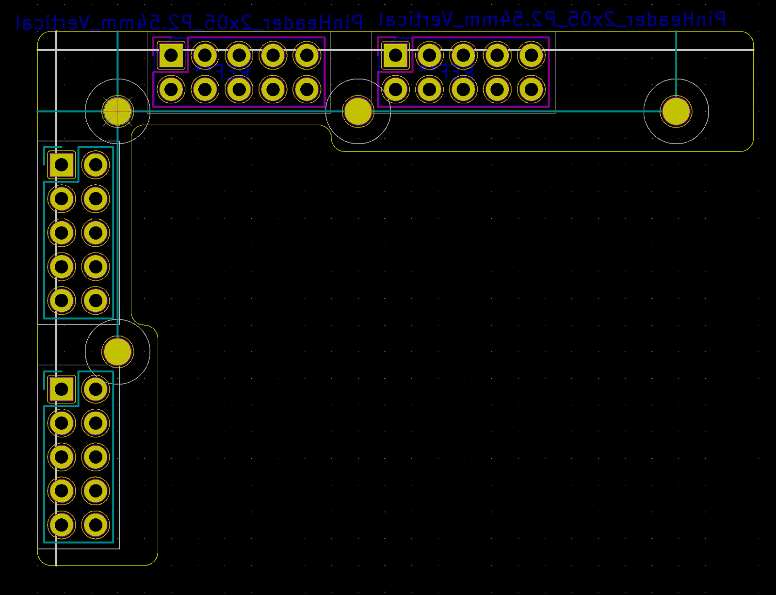
KiCAD is a great PCB design tool, but terrible for mechanical drawings. There was no time, however, to learn something else. The 4 circles match exactly the location of mounting holes in the LED matrix panel, and the different width indents are necessary to avoid various components on the panel.
I used kicad-util to add mouse bites and bridges between multiple instances of the same corner bracket. It takes a bit to learn how it works, and the error messages aren’t always helpful, but it was very useful once I got the hang of it. Checkout this file that I used as input to kicad-util.
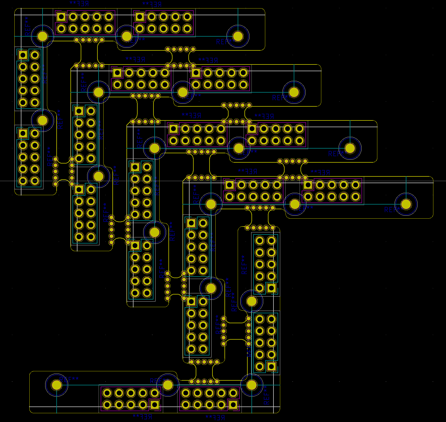
With 5 corners per PCB and 10 PCBs ordered, I had 50 corners, double the 24 that I needed:
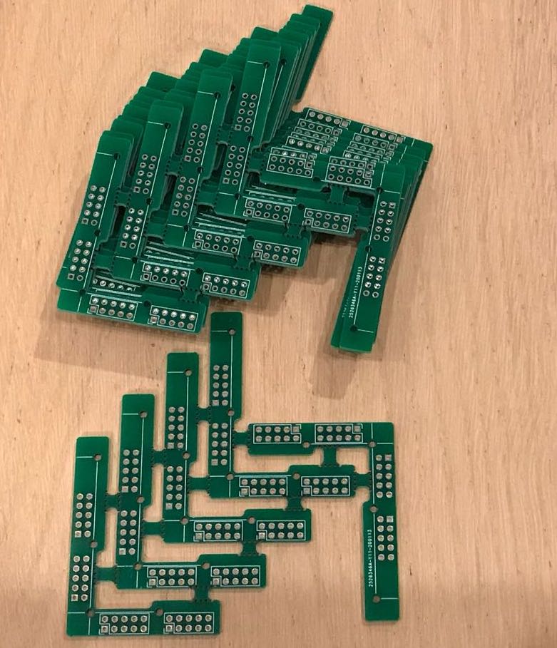
Cube Assembly - First Try
When the corner piece PCBs arrived, I could try the first assembly.
There were good points:
- the location of the mounting holes and the PCB drill holes matched perfectly. My calipers had done a great job!
- the general concept of making corner pieces worked, in general. It was possible to assemble all 12 LED panels and create a self-sustaining structure, as long as you oriented the panels the right way.
But also some bad ones:
- the location of the pin header holes in combination with the 90 degree pin headers themselves resulted in huge unsightly seams between the panels.
- the 2 panels on the same surface weren’t linked together. They were very easy to shift, which made things even uglier (see red rectangle below, and that wasn’t the worst example.)
Cube Assembly - Second Try
For the first assembly, I was using double-row 90 degree headers. I figured that switching to a single row would go a long way in reducing the gap.
Much better! At least the gap between the PCBs of the corner brackets are gone. It’s still not perfect: even if the PCBs touch each other on the inside, the thickness of the PCB itself means that there’s a gap on the outside.
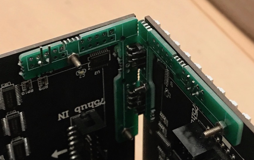
To fix that, I’d have to move the mounting holes on the corner brackets more towards the corner. But there was no time for a redesign, so I just went with what I had. I had to scrap the 8 corner pieces that I had already made, but I had ordered enough PCBs for a second set. Phew!
The problem of linking the 2 panels on the same surface was unexpectedly solved by observing that the mounting holes on one leg of the corner bracket were spaced exactly right. I could reuse the scrapped pieces for that.
Tying the 2 panels together worked wonders. The cube wasn’t perfect, but it definitely looked decent enough.
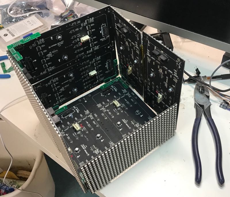
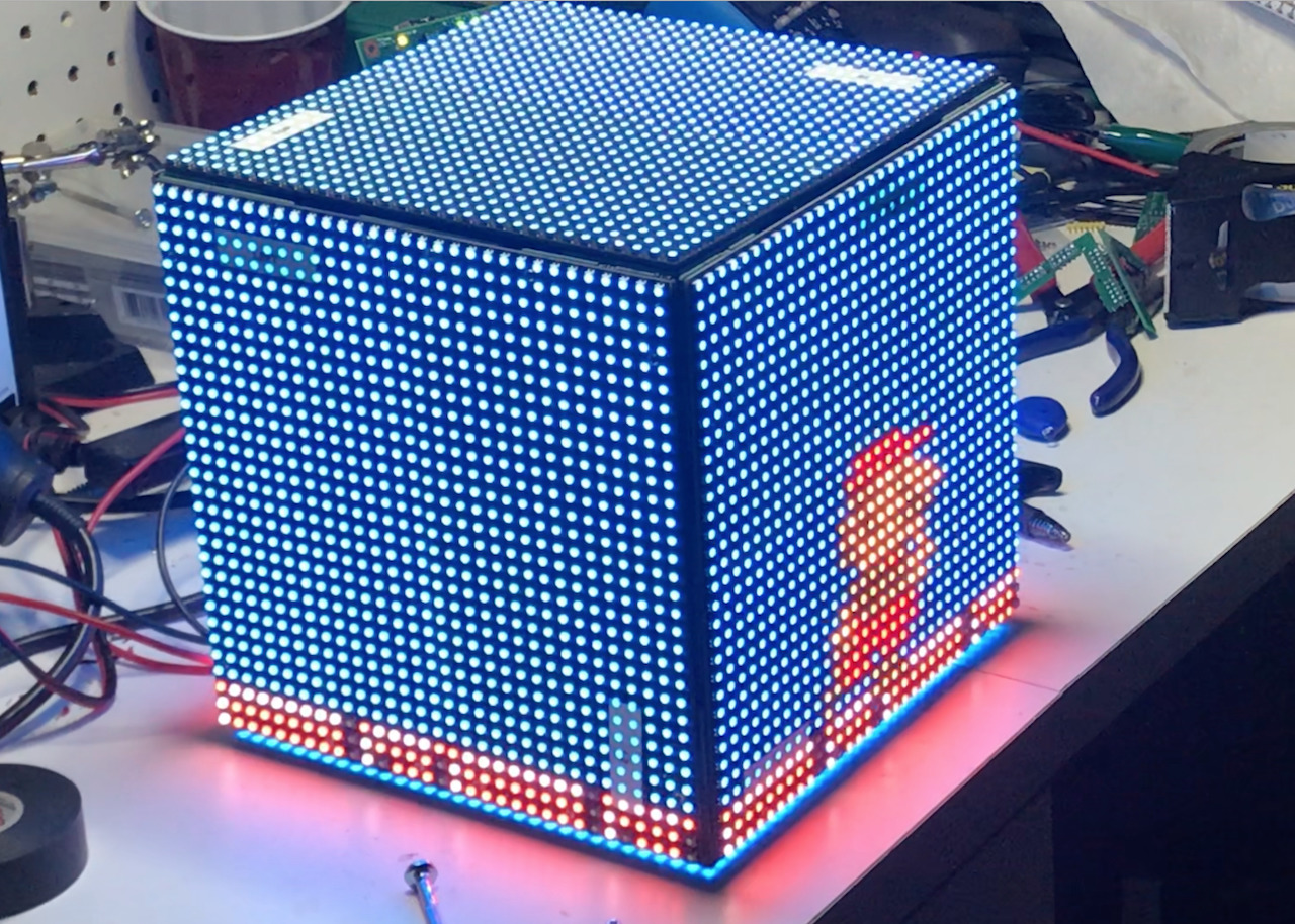
During the project, I had to rebuild the cube multiple times. It was tedious but also satisfying to see it come together. This view gave me a Star Wars Death Star Tunnel vibe:
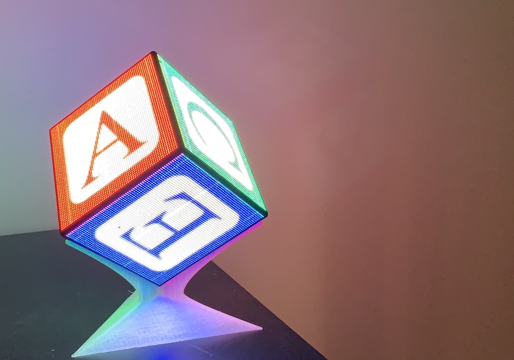
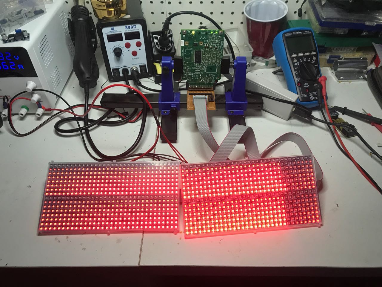
Fully assembled:
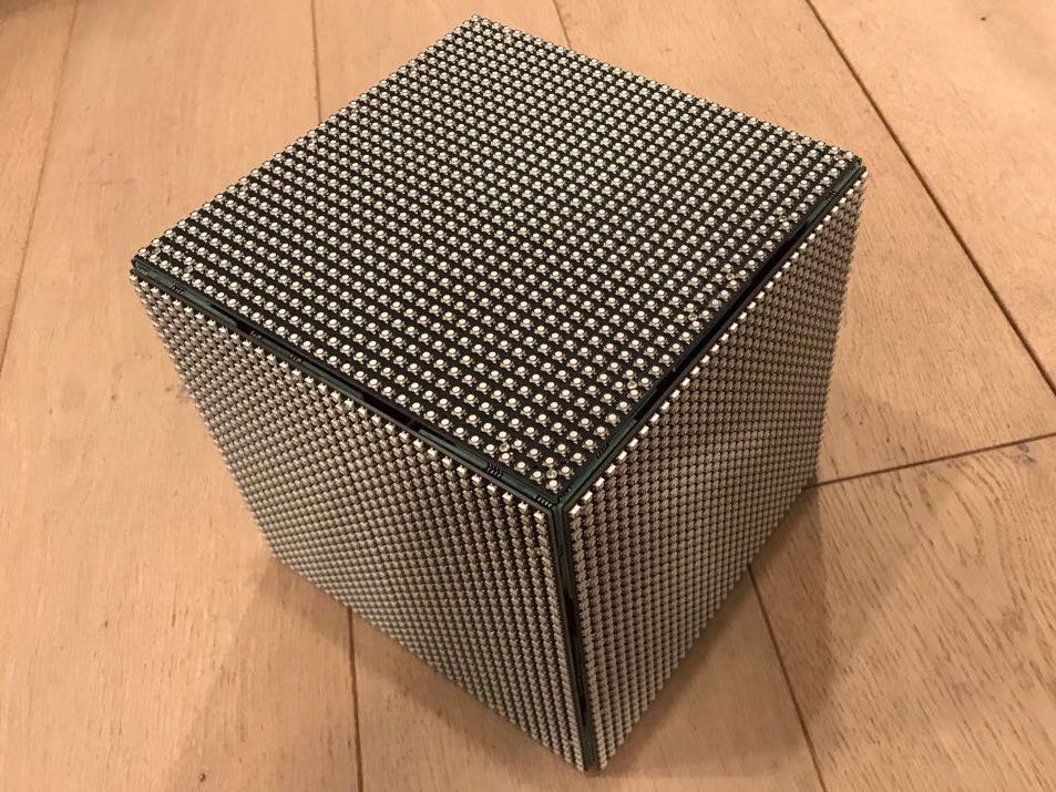
The seams are there, but once lighted up, the animation on the LED panels distracts from the imperfections.
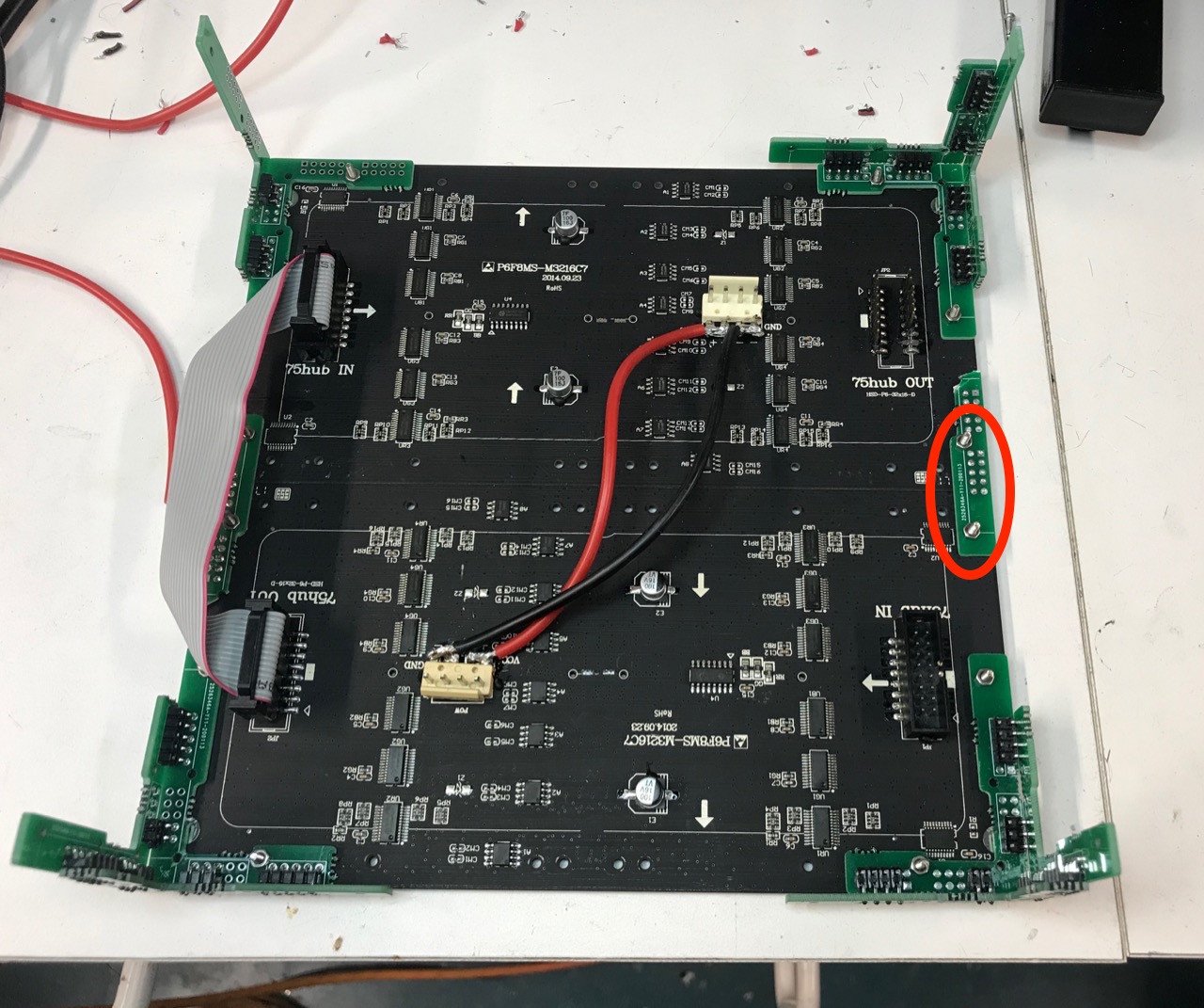
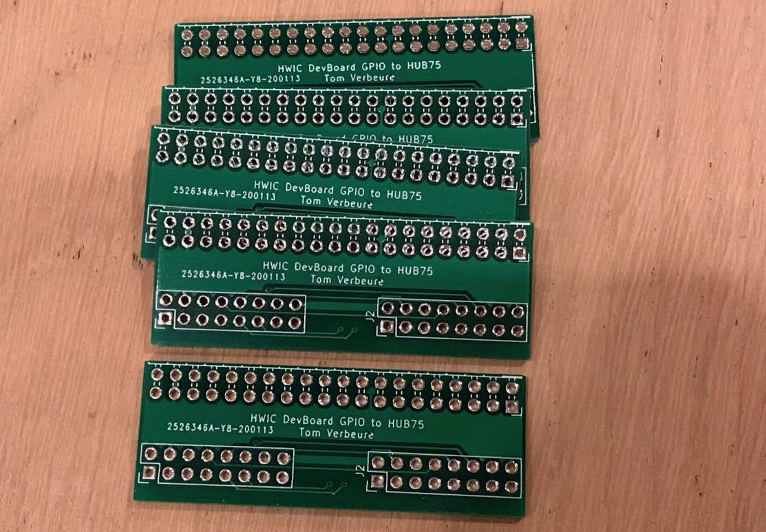
HWIC Interface & HUB75 Adapter Boards
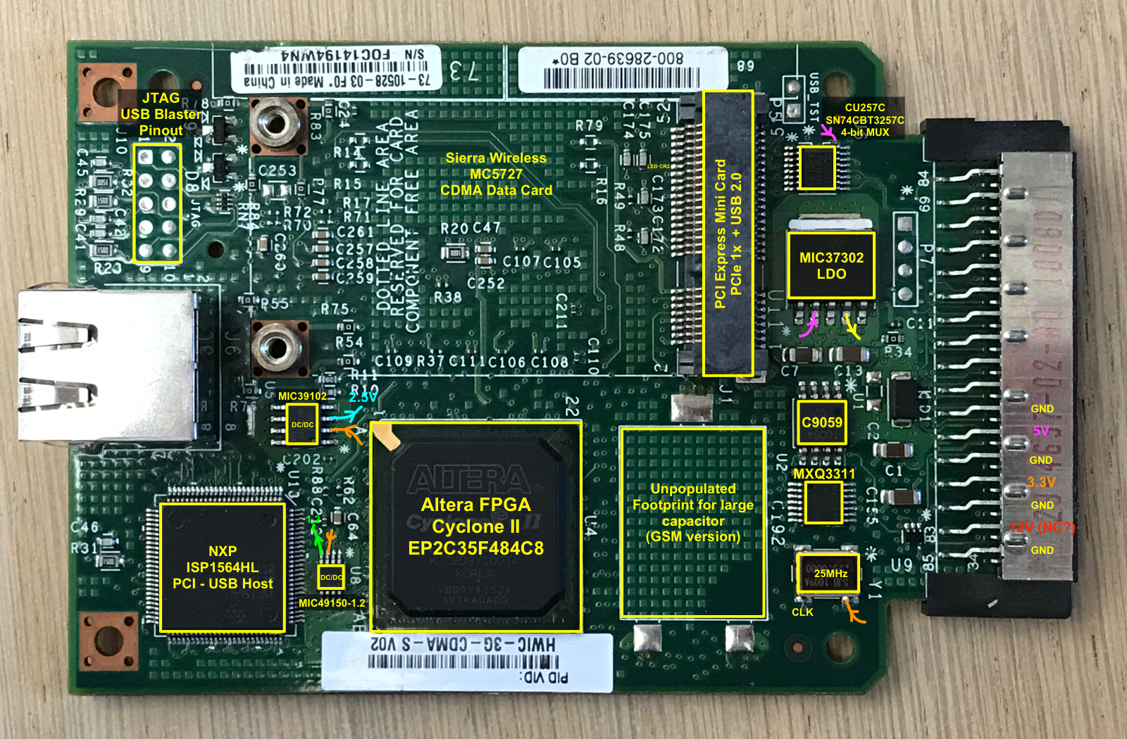
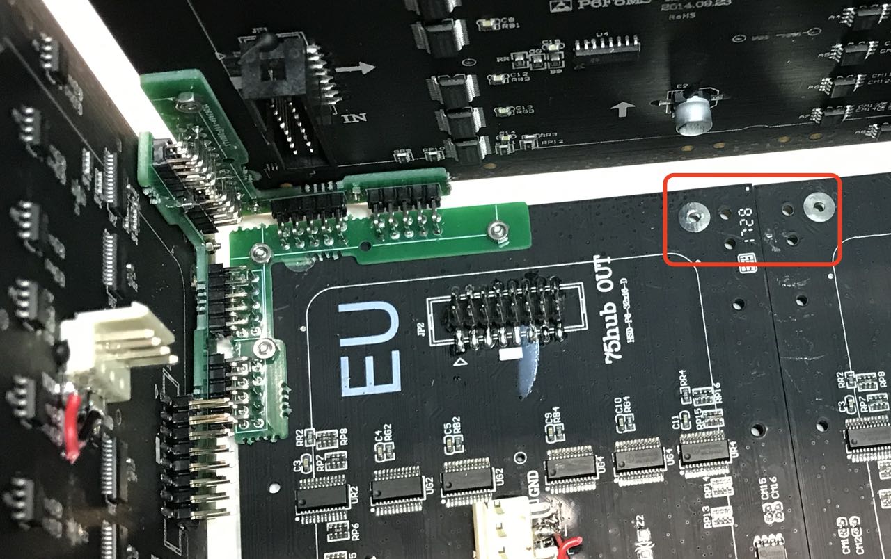
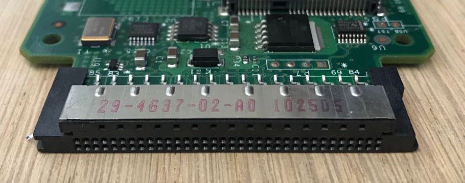
Cisco routers have extension slots for options like WAN ports, modems etc. They use a proprietary HWIC connector that can’t be bought at Digikey or Mouser. On the HWIC-3G-CDMA modem, the HWIC connector has a bunch of GPIOs that route straigth to the Cyclone II FPGA as well as configuration pins that are used to download a bitstream into the FPGA at bootup with the passive serial method.
I needed an interface board with bitstream download logic that plugged into the HWIC connector.
The HWIC connector has 1 row for pins that are spaced 2.54mm apart, just like standard pin headers. This row is used to supply power to the board. There are also 2 rows for pins that are spaced 1.27mm apart. These contain the IOs.
My earlier prototype used a soldered board with only one row of 1.27mm pins and with 50% of the pins in that row removed. That wasn’t enough to drive a full HUB75 interface, which is why my earlier picture only had red LEDs lighting up!
With a PCB, I’d be able to connect all the pins that I needed:
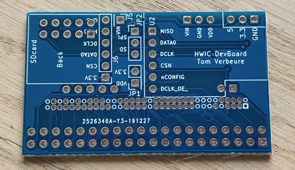
In addition to the 3 rows with pins, there’s a room to connect an SDcard and an ATtiny to manage downloading a bitstream from the SDcard into the FPGA.
Unfortunately, minutes after receiving the boards on New Year’s Eve, I found out that I had swapped around the 2.54mm row and the 1.27mm rows!
I was able to salvage the board by soldering the pins on the other side. This gave me enough GPIO pins to drive a full HUB75 interface.
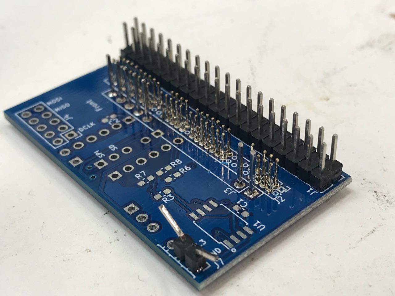
The interface board routes the 1.27mm GPIO pins to a traditional double row 2.54mm pin header. I wanted the board to be general purpose, so the pin header wasn’t laid out in a HUB75 configuration. An additional adapter PCB took care of that:
It arrived on January 16th, together with the fixed HWIC interface board.
Hot Tip: when you spin different revisions of a board, uses different PCB colors for each revision to avoid using the wrong version!
Overall FPGA Digital Design
All this hardware needs smarts to drive the right timing to the LED panels.
By now, you should know that these panels use a relatively standard HUB75 protocol. I could spend a lot of words describing the details of this protocol, but Glen Akin’s tutorial already does that very well.
The most important part to remember is that it uses 1-bit per color component (3 bits per pixel) and that it shifts the values of 1 or 2 rows (depending on the panel type) of the matrix into a shift register which then gets displayed.
It’s up to the driving logic to continuously refresh the LED rows to give the impression that all LEDs are lighted up at the same time. And if you want more than just 1 color per component, you need to do it even faster and create the right intensity with pulse-length modulation.
I love writing RTL, so there was no way I’d reuse somebody else’s code for that! As always, I used SpinalHDL, my RTL language of choice for all my hobby projects.
Here’s the architecture that I came up with:

The VexRiscv CPU is responsible for creating interesting images that get written in a double buffered LED frame buffer RAM.
The HUB75 Streamer fetches the pixels in the correct order (see below), sends them through a gamma correction lookup table, dims them, and demuxes them into 2 parallel streams, and finally sends it to a burst output FIFO that is deep enough to cover 2 rows. This is needed to buffer up enough pixels when the LSBs of the pixels are sent out: they are scanned at double the rate at which pixels are fetched from the RAM.
The HUB75 Phy receives the pixels from the streamer and sends them out with the correct low level HUB75 protocol and timing.
The gamma correction is very important: not only does it make sure that color gradients look right to our eye, it also pushes more LED values to a lower intensity. LEDs consume a ton of power, so this is an important battery saving step.
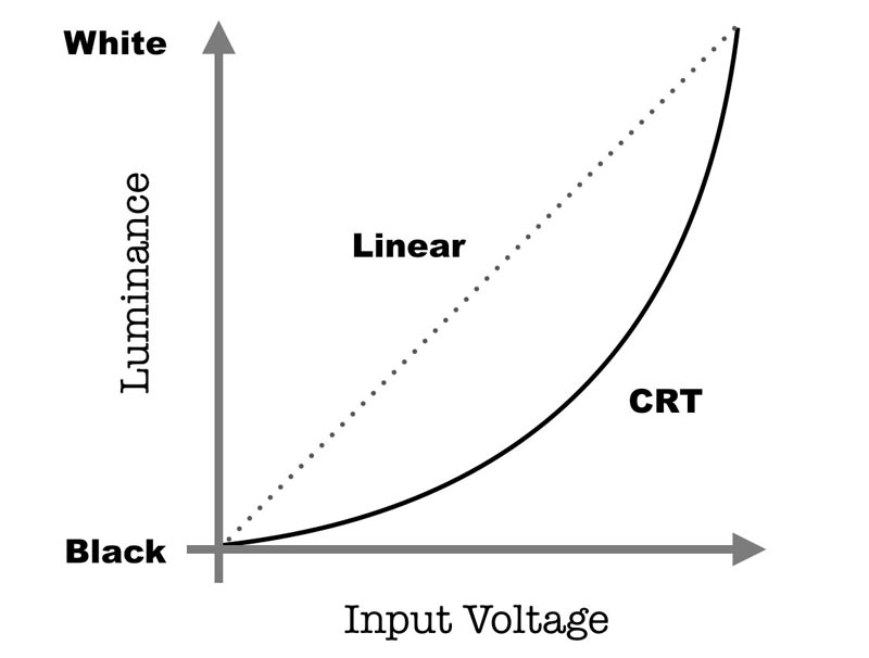
The same is true for the dimming function: it simply multiplies all pixel values to a smaller value.
The CPU could do this in software, but both functions are trivial to implement in hardware, and doing so frees up a lot of cycles on the 50MHz CPU.
Correcting for Panel Orientation and Location in the HUB75 Streamer
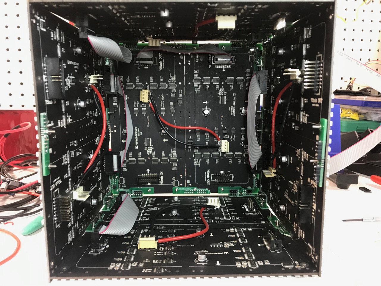
The LED panels were assembled in such a way that the internal cabling was as straightforward as possible. You can see a bit of that in the Death Star picture earlier, but that doesn’t show interconnecting different sides of the cube. There’s a rats nest of cables in the end!
An optimal cabling results in LEDs locations aren’t located in the most logical position from a software point of view: there are different orientations and rotations for each of the 16 LED panels.
I wanted software to be as easy as possible. That’s why the LED RAM has the LED locations in a logical order that’s easy to use for the software. The address generation part of the streamer is responsible to fetch the LED values in a order that matches the physical arrangement.
This is one of those things where SpinalHdl shines. Here is the hardware structure that configures the scan order of LEDs:
case class PanelInfoHW(conf: Hub75Config) extends Bundle {
    val topLeftXCoord           = SInt(2 bits)
    val topLeftYCoord           = SInt(2 bits)
    val topLeftZCoord           = SInt(2 bits)

    val memAddrStartPh0         = UInt(log2Up(conf.total_nr_pixels+1) bits)
    val memAddrStartPh1         = UInt(log2Up(conf.total_nr_pixels+1) bits)
    val memAddrColMul           = SInt(log2Up(conf.panel_cols)+2 bits)
    val memAddrRowMul           = SInt(log2Up(conf.panel_cols)+2 bits)

    val xIncr                   = SInt(2 bits)
    val yIncr                   = SInt(2 bits)
    val zIncr                   = SInt(2 bits)
}
And here are the actual values for the 12 panels:
    val panels = ArrayBuffer[PanelInfo]()

    //                topLeftCoord   Side  Top      Rot    xyzIncr
    panels += PanelInfo(-1, 1,-1,       5, true,    0,     0,-1, 1)
    panels += PanelInfo(-1, 0,-1,       5, false,   0,     0,-1, 1)

    panels += PanelInfo(-1, 1,-1,       4, true,    0,     1, 0, 1)
    panels += PanelInfo(-1, 1, 0,       4, false,   0,     1, 0, 1)

    panels += PanelInfo(-1,-1, 1,       3, true,    0,     1, 0,-1)
    panels += PanelInfo(-1,-1, 0,       3, false,   0,     1, 0,-1)

    panels += PanelInfo( 1, 1,-1,       2, true,    0,    -1,-1, 0)
    panels += PanelInfo( 1, 0,-1,       2, false,   0,    -1,-1, 0)

    panels += PanelInfo( 1, 1, 1,       1, true,    90,    0,-1,-1)
    panels += PanelInfo( 1, 0, 1,       1, false,   90,    0,-1,-1)

    panels += PanelInfo(-1, 1, 1,       0, true,    180,   1,-1, 0)
    panels += PanelInfo(-1, 0, 1,       0, true,    0,     1,-1, 0)
After changing these configuration parameters too many times, and getting tired of waiting for synthesis results, I made these configuration parameters programmable by the CPU. That way, I could use the fast update memory update hack that I described in a recent blog post.
From One to Two HUB75 Ports
For simplicity, my initial plan was to use 1 HUB75 port.
That worked great for 8 panels, but I started seeing corruption on the 9th LED panel.
I didn’t put the signal on an oscilloscope to confirm, but I’m pretty certain that there were timing issues after sending clock and data through too many ribbon cables. By doubling the number of interfaces, both the length of the chain and the shift clock speed could be reduced by half.
This shows that committing to a talk without working out all the details first carries significant risk: adding a second HUB75 interface exhausted all the available GPIOs on the HWIC interface!
Rick, Pac-Man, Mario
“Never Gonna Give You Up” may not be the Hello World of moving images, Bad Apple probaby holds that title, but it’s close.

I found a GIF with his smooth moves, and created a post-processing pipeline that does the following:
- Start with
rick_orig.gifwhich contains multiple images. - Resize to 32x23 pixels so that everything fits in a 32x32 LED matrix.
- Extract all individual PNG images.
- Join all images into 1 image.
- Reduce the colors of the joined image to a palette of only 16 colors
- Map all individual images to 4 bits per pixel palette to save memory
- Save images as pure binary files
- Concat all the binaries to one binary file
- Convert this bin file to a C include file which can be included directly into the C code that runs on the VexRiscv CPU.
This is all done in a Makefile that you can find here.
Here’s Rick in all his resolution reduced glory:
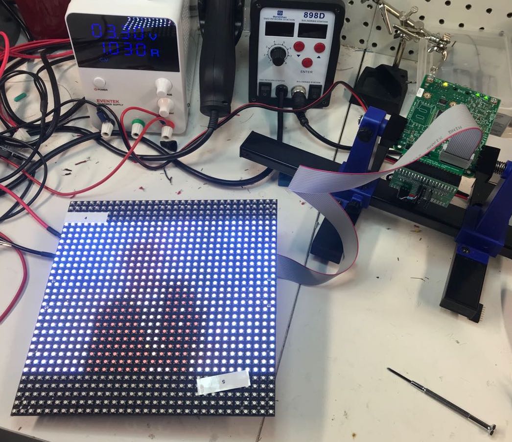
Notice how all the bright LEDs pull a 1A at 3.3V, good for 3.3W. Dialing down brightness is essential to make everything work on a triplet of AA batteries!
You can also see the tags “4” and “5” taped on the panel. They are taped with the right orientation and location to make it easy to remember the panel configuration parameters.
The resolution is obviously very low, when looking at it from a few meters, and with animation enabled, it’s undeniably Rick.
A single animation would be a bit poor, so I added Pac-Man chasing and being chased by ghosts:
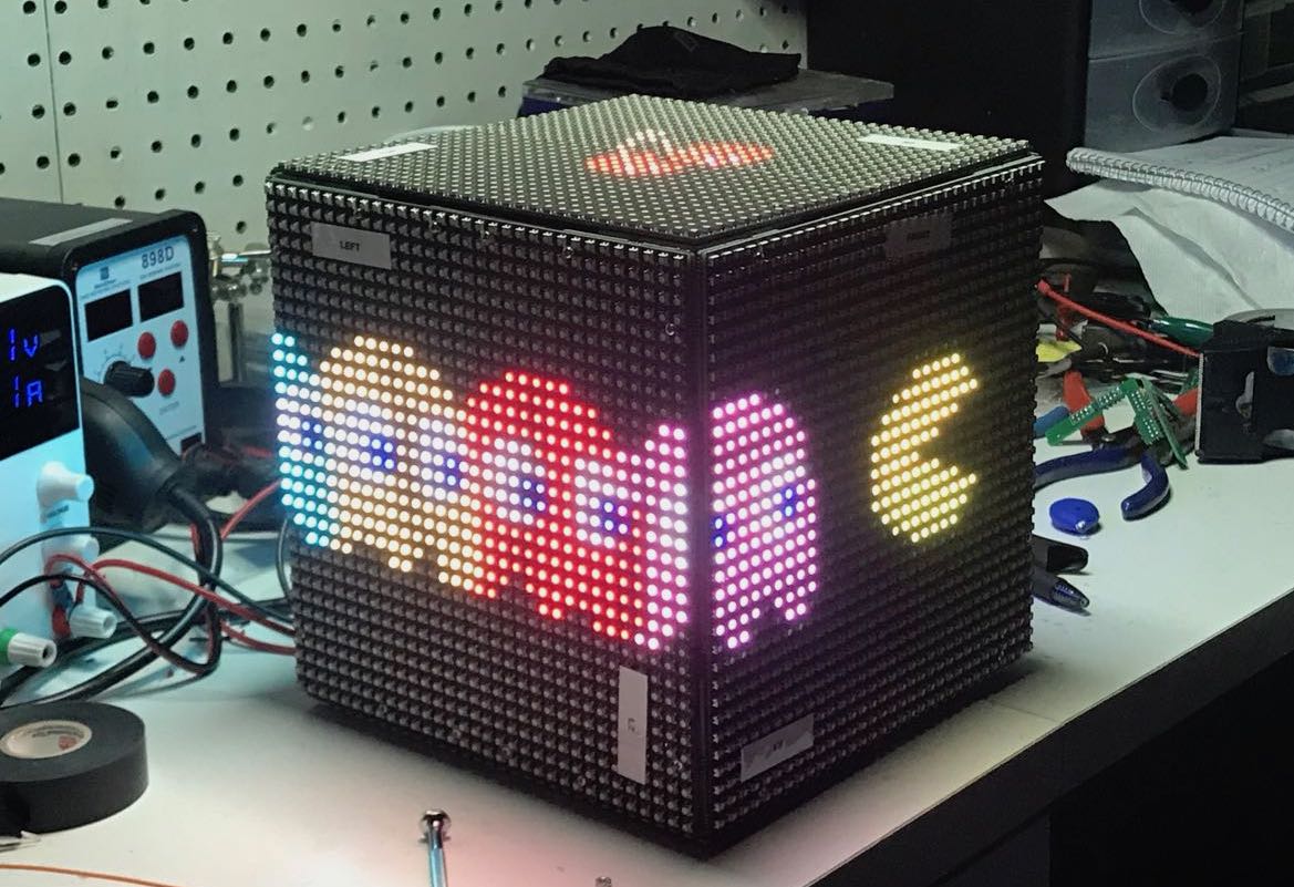
And Mario running around aimlessly with nothing else to do:
The bitmaps use either 2 or 4 colors and are defined as binary structs in the main C code:
uint32_t ghost_left_0[14] = {
    0b0000000000010101010000000000,
    0b0000000101010101010101000000,
    0b0000010101010101010101010000,
    0b0001010101010101010101010100,
    0b0001010111110101010111110100,
    0b0001011111111101011111111100,
    0b0101011111101001011111101001,
    0b0101011111101001011111101001,
    0b0101010111110101010111110101,
    0b0101010101010101010101010101,
    0b0101010101010101010101010101,
    0b0101010101010101010101010101,
    0b0101010100010101010001010101,
    0b0001010000000101000000010100,
};
If you didn’t know that GCC supports binary constants, you do now!
This is the final result:
Unexpected Short Circuits Solved with UV Hardened Glue
After yet another assembly, I noticed that some LED panels would stop functioning correctly by holding it the wrong way.
This was quickly root caused as a short circuit. The head of the bolts that tie the corner pieces to the LED panel would sometimes touch multiple LED pins at the same time.
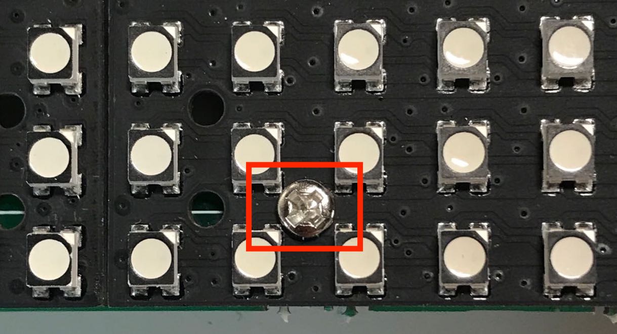
I could have used plastic nuts and bolts instead, but lacking those, I used UV hardening glue on each bolt to create an insulation layer.
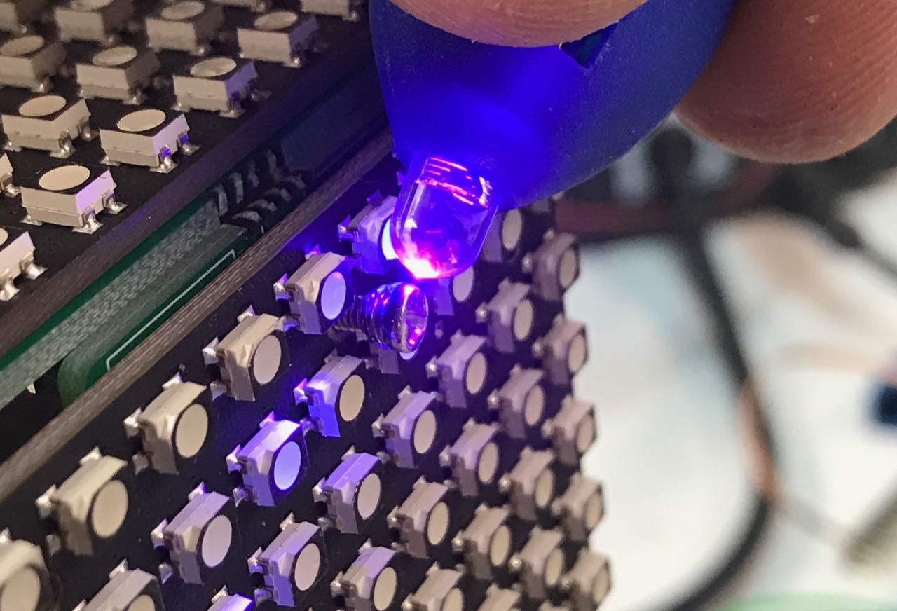
These glues sell for just a couple of dollars on AliExpress or Amazon and despite the terrible chemical smell, they’re awesome. I use them all the time to hold delicately soldered wires in place on a PCB.
The only issue was the tedium of adding this insulating layer on all the bolts: there are 96 of them!
Powering the Cube
I used 3 AA battery to generate 4.5V and used one of those dirt cheap LM2596-based step-down regulator modules.
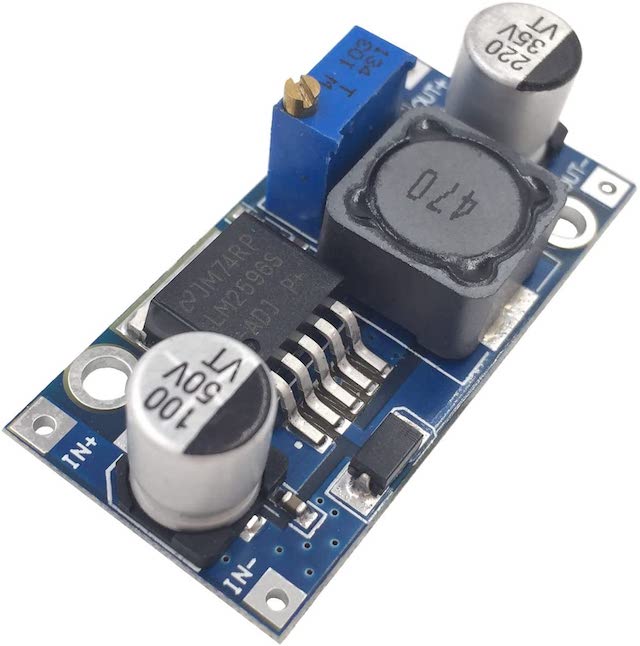
The modem has its own voltage regulators to convert this 3.3V further down to the needs of the FPGA.
LED matrix panels require a 5V supply, but they usually work just fine on 3.3V too. In additional to reduced power consumption, another benefit was not needing level shifters to convert the 3.3V FPGA IOs to 5V.
Integrating It All and Shortcuts
There are a few practical questions that still need to be answered:
-
How to secure the electronics inside the cube?
The answer to that is simple: I didn’t. There are so many cables inside that you can just wrap the Cisco modem inside a carton box and stuff in the the cube and it will remain suspended among all the mess as long as you don’t shake too hard.
This would be a terrible idea if you were planning to travel with it on an airplane, but it was good enough for a one-time demonstration.
-
What about batteries and how do you switch it on and off?
Switching the thing on and off was linked to ‘solving’ the battery issue: I just had 2 wires going out of the cube through the seams and connected them to the batteries when I had to light it up.
Not elegant at all, but it was once again good enough.
-
How do you open the cube?
By having the bolts inside-out for the top panel. Opening the cube is a matter of unscrewing 16 tiny nuts.
I also took a shortcut to configure the FPGA: I didn’t finish the subproject of loading the bitstream from an SDcard and loading it into the FPGA with the ATtiny of the HWIC interface board.
Instead, I had a USB-Blaster ribbon cable handing out off the bottom of the cube. After powering up the cube, I’d quickly use a laptop and Quartus to download the bitstream into the FPGA. I practiced this manouver a couple of times, and it went without a hitch during the presentation.
Presenting at !!Con West
It’s crazy to think how COVID naive we still were on that March 1st, 2020: while we were advised to not shake hands (“practise vigorous hand waving instead”), there wasn’t a mask to be seen. A week later the whole country would shut down.
The presentation went very well! I’m not a confident public speaker, but having a welcoming audience makes all the difference.
I spent quite some time on the low cost of PCBs, and how to use that to your advantage when making mechanical designs, since that’s probably not well known with a computer science oriented audience.
Looking Back…
The whole project was a success. My second major hobby project after my Racing the Beam Ray Tracer (which I presented at !!Con West 2019.) I look back at it fondly!
From start to finish, it took me about a month: the last code change “Mario” was committed to GitHub on January 26st. While that gave me plenty of time to make improvements, that day was also the start of a major house remodel that made us camp out in the garage that’s also my home electronics lab.
Looking back, there were a lot of things that could have gone bad:
-
I had no spare LED matrix panels.
Those bolt induced short circuits should have easily damaged multiple boards.
-
COVID-related PCB supply issues
A month later, and PCBs from China were almost impossible to get because everybody switches to making medical equipment and because transportation to the US was halted.
-
Needing 2 HUB75 interfaces instead of 1
I literally had no GPIOs left after making that switch…
In the end, none of that happened. But the overall lesson is clear: Don’t commit to a conference talk with an unrealised idea!
There’s some desire to clean up the loose ends at some point: the HWIC interface board would be better with a PMOD interface, I want the bitstream loader to work, and a particle simlation guided by an accelerometer isn’t very original, but it looks so incredibly cool.
But I doubt that these will ever happen. There are so many interesting project to be done, and this one has largely run its course.
References
-
LED Cube project on GitHub
-
Panelization, mouse bites etc.