A Hack to Update RAM Initialization Contents in Intel FPGA Bitstreams
- Introduction
- The Generic Way to Infer Initialized RAMs
- Manual Instantiation of Intel Block RAMs
- Fast Bitstream Update after Changing a MIF File
- Fast Bitstream Update for the Generic Verilog Case
- Mini CPU: A Concrete Design Example
- Conclusion
Introduction
The logic elements of FPGAs are configured with a bitstream: lookup tables of logic elements get the content that defines their behavior, switches on interconnect networks create the desired routing topology, flip-flops are connected to the right clock network, etc.
Most FPGAs also allow block RAMs to be given a non-zero content during configuration.
This is an essential feature when the FPGA has a soft-core CPU, because it’s the easiest way to have boot code present immediately after powering up.
In my personal projects, I often use tiny CPUs to implement controllers for all kinds of low speed protocols like I2C, SPI, Ethernet PHY MDIO etc. In those cases, all the firmware is pre-baked in block RAMs. I hardly ever use external flash to store firmware: the amount of C code that I usually need is just not large enough.
Using tiny CPUs instead of hardware also allows for rapid iteration: if you can avoid the process of synthesis and place-and-route, and replace it by compile-firmware and update-bitstream, you can save minutes in iteration time for tiny designs, or hours for large ones.
Which brings up to the question:
How can you quickly update bitstreams with new RAM content without going through resynthesis and place-and-route?
In this blog post, I’ll describe 2 techniques:
- the official one, which requires hand-instantiation of an Intel FPGA RAM model and using a HEX or a MIF file.
- a hack that allows using Verilog inferred RAMs in Verilog that are initialized
with
$readmem(...).
The first option uses an Intel altsyncram primitive and doesn’t work with FPGAs of
vendors. The second option makes the RTL of your design compatible across different FPGA families.
I also have an example where both techniques are implemented in a minimal but useful CPU system.
The Generic Way to Infer Initialized RAMs
The generic way to add RAM to your FPGA design looks more or less like this:
    localparam mem_size_bytes   = 2048;

    // $clog2 requires Verilog-2005 or later...
    localparam mem_addr_bits    = $clog2(mem_size_bytes);

    reg [7:0] mem[0:mem_size_bytes-1];

    wire                     mem_wr;
    reg [mem_addr_bits-1:0]  mem_addr;
    reg [7:0]                mem_rdata;
    reg [7:0]                mem_wdata;

    always @(posedge clk)
        if (mem_wr) begin
            mem[mem_addr]   <= mem_wdata;
            mem_rdata       <= mem_wdata;       // Some Intel FPGA RAMs require this...
        end
        else
            mem_rdata  <= mem[mem_addr];
Any competent FPGA synthesis tool will infer a 2KB block RAM from the code above.
If you want the RAM contents to be initialized after configuration, just add the lines below:
    initial begin
        $readmemh("mem_init_file.hex", mem);
    end
This method works for simulation and, once again, most competent FPGA tools will synthesize a bitstream that initializes the block RAM with content after configuration. (ASIC people won’t like it at all, though!)
An important observation here is that during the whole process from RTL to bitstream,
the FPGA tool will process the $readmemh() statement during RTL analysis and
synthesis. These steps happen at the front of the whole bitstream creating process.
As a result, a dumb implementation will require restarting the process at that point
when you change the contents of mem_init_file.hex. At least, that’s how it
is for Quartus… (The open source ICE40 and ECP5 synthesis and P&R tools don’t fall
in the dumb implementation category!)
There must be a better way…
Manual Instantiation of Intel Block RAMs
Instead leaving it up to the synthesis tool to infer RAMs out of generic behavioral Verilog, you can also explicitly instantiate RAM primitives in your code. This can be useful for a variety of reasons.
One reason is when you want to exploit very specific features of a particular FPGA’s block RAM.
A common case is where I want to make sure that my block RAM has flip-flops both at the input of the RAM (address, write data, write enable) and at the output (read data.)
This increases the read latency of the RAM from one to two cycles, but in many designs that’s not an issue, and it can result in significant clock speed improvements.
In the code below, there’s a pipeline stage on the output of the RAM, which is then used as an operand of a multiplier:
    reg [7:0] mem[0:mem_size_bytes-1];

    always @(posedge clk)
        if (mem_wr_p0) begin
            mem[mem_addr_p0] <= mem_wdata_p0;
            mem_rdata_p1     <= mem_wdata_p1;
        end
        else
            mem_rdata_p1     <= mem[mem_addr_p0];

    // Additional pipeline stage to break timing path between RAM and multiplier input
    always @(posedge clk)
        mem_rdata_p2    <= mem_rdata_p1;

    always @(posedge clk)
        result_p3       <= some_other_data_p2 * mem_rdata_p2;

For cases like this, FPGA RAM inference can be hit-and-miss, because the synthesis tool has 2 implementation options
for the rd_data_p2 register.
It could use the output FFs of the RAM. Like this:

Or it could use the input FFs of the DSP block. Like this:

When I want fine control in situations like this, I instantiate the RAM by hand with an Intel RAM primitive cell. The earlier behavioral RTL code is converted to something that’s partly structural:
    // altsyncram is an Intel primitive for all synchronous RAMs.
    // It has tons of tweaking options...

    altsyncram #(
        .operation_mode    ("SINGLE_PORT"),
        .width_a           (8),
        .width_ad_a        (mem_addr_bits),
        .outdata_reg_a     ("REGISTERED")           // <<<<<<<<<<
    )
    u_mem(
        .clock0   (clk),
        .address_a(mem_addr)
        .wren     (mem_wr),
        .data_a   (mem_wdata),
        .q_a      (mem_rdata_p2)
    );

    always @(posedge clk) begin
        result_p3 <= some_other_data_p2 * mem_rdata_p2;
    end
The marked line is key here: using “REGISTERED” enables the output FFs of the RAM and adds the additional pipeline stage.
The new code can’t be used with FPGAs of other vendors, and even simulating it is a hassle, because Intel simulation models are usually encrypted and only work with commercial Verilog simulation tools like ModelSim or VCS.
My workaround for that is to have an ifdef that selects behavioral Verilog for simulation,
and altsyncram for synthesis.
The altsyncram primitive also has the optional init_file parameter:
    altsyncram #(
        .operation_mode    ("SINGLE_PORT"),
        .width_a           (8),
        .width_ad_a        (mem_addr_bits),
        .outdata_reg_a     ("REGISTERED"),
        .init_file         ("mem_init_file.mif")    // <<<<<<<<<<
    )
    u_mem(
        ...
MIF stands for “Memory Initialization File”. It’s an Intel proprietary text file format
to, well, initialize memories. I use my own
create_mif.rb script
to convert binary files into a MIF files.
It’s possible to use Verilog inferred RAMs with MIF files:
(* ram_init_file = "mem_init_file.mif" *) reg [7:0] mem[0:mem_size_bytes-1];
But this construct makes simulation even more problematic: simulators
don’t know what to do with the Intel-specific ram_init_file attribute, so they
just ignore it!
Fast Bitstream Update after Changing a MIF File
The beauty of using an altsyncram and a MIF file is that you can easily update
your bitstream after changing the MIF file without starting out from scratch.
Just perform the following steps:
-
Change the MIF file with the new contents
-
Quartus GUI: Processing -> Update Memory Initialization file
This loads your updated MIF file into the Quartus internal design database.
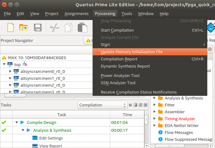
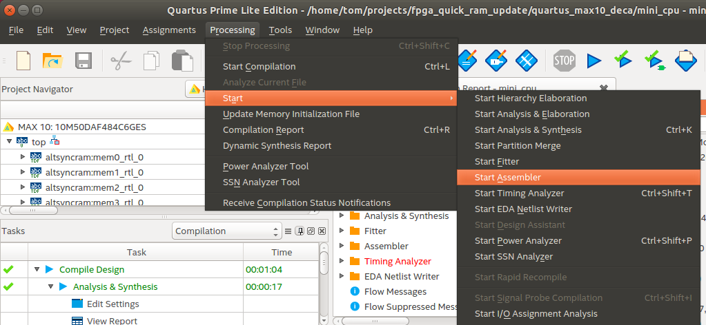
-
Quartus Gui: Processing -> Start -> Start Assembler
This creates a bitstream from the Quartus internal design database.
Instead of using a GUI, I use a Makefile to do the 2 Quartus steps:
QUARTUS_DIR = /home/tom/altera/13.0sp1/quartus/bin/
DESIGN_NAME = my_design

update_ram: sw
	$(QUARTUS_DIR)/quartus_cdb $(MY_DESIGN) -c $(MY_DESIGN) --update_mif
	$(QUARTUS_DIR)/quartus_asm --read_settings_files=on --write_settings_files=off $(MY_DESIGN) -c $(MY_DESIGN)

sw:
	cd ../sw && make
The sw rule builds the latest firmware version and creates the new MIF file. quartus_cdb updates
the design database, and quartus_asm creates the new bitstream.
Fast Bitstream Update for the Generic Verilog Case
To update inferred RAMs that were initialized with $readmemh(), we need to hack
the Quartus design database ourselves. This is easier than you’d think because Quartus uses the MIF file format
in that database!
The steps to update your inferred RAMs are as follows:
-
find the MIF file in the database that’s used for your RAM
I do this by listing all the MIF files in the database:
cd quartus/db ll *.mif -
create a MIF file for the inferred RAM
In the makefile for my firmware, I always immediately build both a HEX file (for use by
$readmemh()) and MIF file. - copy your MIF file over the MIF file in the internal database
- do the earlier 2 Quartus steps
The Makefile looks like this:
QUARTUS_DIR = /home/tom/altera/13.0sp1/quartus/bin/
DESIGN_NAME = my_design

DB_MEM_MIF  = $(wildcard ./db/*mem*.mif)
SRC_MEM_MIF = ../sw/mem_init_file.mif

update_ram: sw $(DB_MEM_MIF)
	$(QUARTUS_DIR)/quartus_cdb $(MY_DESIGN) -c $(MY_DESIGN) --update_mif
	$(QUARTUS_DIR)/quartus_asm --read_settings_files=on --write_settings_files=off $(MY_DESIGN) -c $(MY_DESIGN)

$(DB_MEM_MIF): (SRC_MEM_MIF)
	cp $< $@

sw:
	cd ../sw && make
The key part here is selecting the correct MIF file in the database. The name of this file will match the hierarchy of where the memory lives in design, but there will also be some random hexadecimal suffix.
When you have multiple RAMs that must be updated this way, you need to be a bit careful about making the wildcard right, but it’s really not very difficult.
Mini CPU: A Concrete Design Example
To illustrate the concepts that I’ve described here, I created a small but non-trivial example that contains a VexRiscv CPU, dual-ported RAM to store CPU instructions and data, and some peripheral registers to control LEDs and read an button. You can find its GitHub repo here.
The example has been tested on my Arrow DECA FPGA board, but it’s easy to port it on other Intel FPGA boards.
There’s a `define
to select between generic RAM inference
and altsyncram instantiation.
The Makefile
in the ./quartus_max10_deca directory shows how to update the 4 RAMs that contain the firmware.
Give it a try when you have an DECA board:
- compile the firmware in the
./swdirectory - create a bitstream
- verify that the LEDs are rotating in one direction
- change a define in the firmware to make the LEDs rotate in the opposite direction
- Do
make update_ramin the./quartus_max10_decadirectory to update the bitstream without recompilation.
If you have a different Intel based FPGA board, copy the ./quartus_max10_deca directory, and make it work. I’m
ready to accept pull requests.
Conclusion
I’ve been using this technique for a couple of years now. The reduction in iteration time is significant and a big stimulus to move even more non-timing critical functionality from hardware to the CPU.