Reverse Engineering the Cisco HWIC-3G-CDMA
- The Cisco HWIC-3G-CDMA PCB
- An Annotated Overview of the Board
- Powering Up the Board
- JTAG Connector
- And Life There Was!
- LED Blinky
- The Curious Case of Component C9059
- Bitstream Configuration
- Block Diagram: Putting It All Together
- Low Level Connections
The Cisco HWIC-3G-CDMA PCB
After the abandoned attempt (*) to reverse engineer the $5 Cisco VWIC3-2MFT-T1/E1 card (because its Stratix II FPGA is not supported by Quartus Web Edition), I set my sights on another Cisco WAN card, the HWIC-3G-CDMA. This one has a Cyclone II EP2C35F484C8 instead of a Stratix II EP2S30F484C5N, and you better believe that I verified it being supported by the free Quartus version before starting this project!
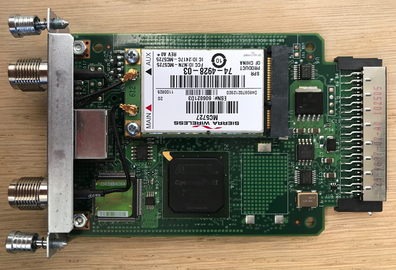
This board is supposed to be inserted in the HWIC slot of a Cisco router and provide WAN functionality, allowing the router to link a local network to the world through a wireless (slow!) CDMA connection.
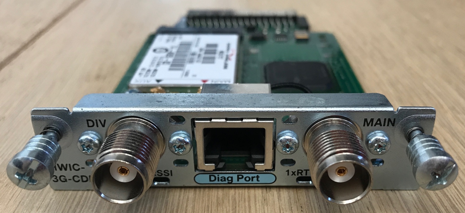
At the front, there are 2 antenna connectors and a diagnostic port. Don’t get too excited about the presence of an Ethernet interface: it’s an RJ-45 port that carries a serial interface using standard RS-232 voltage levels. USB-to-serial-RJ45 cables go for about $10 on Amazon, but they are not required if you have no need for a serial port.
The Cisco marketing documentation mentions all kinds of protocols, but it’s safe to assume that no matter whether or not one of those supported protocols is still in active use, it’ll be very slow, and probably obsolete soon.
At the time of writing this, the cheapest such cards could be bought on eBay for $8, including shipping. As usual, I started out by buying 2, allowing me to destroy one by desoldering components for easier tracing of connections.
I’m not the first one to have a go at this board: the FPGA Board Hack project on Hackaday.io did some work on this as well, but other than a Quartus project on GitHub to blink the LEDs, nothing has been documented: no connections from FPGA to connector, no explanation about how to power the board etc.
This is a pity, because this board has the promise of offering a pretty large, by hobby standards, FPGA with DRAM, for one of the lowest prices around! Let’s correct that!
An Annotated Overview of the Board
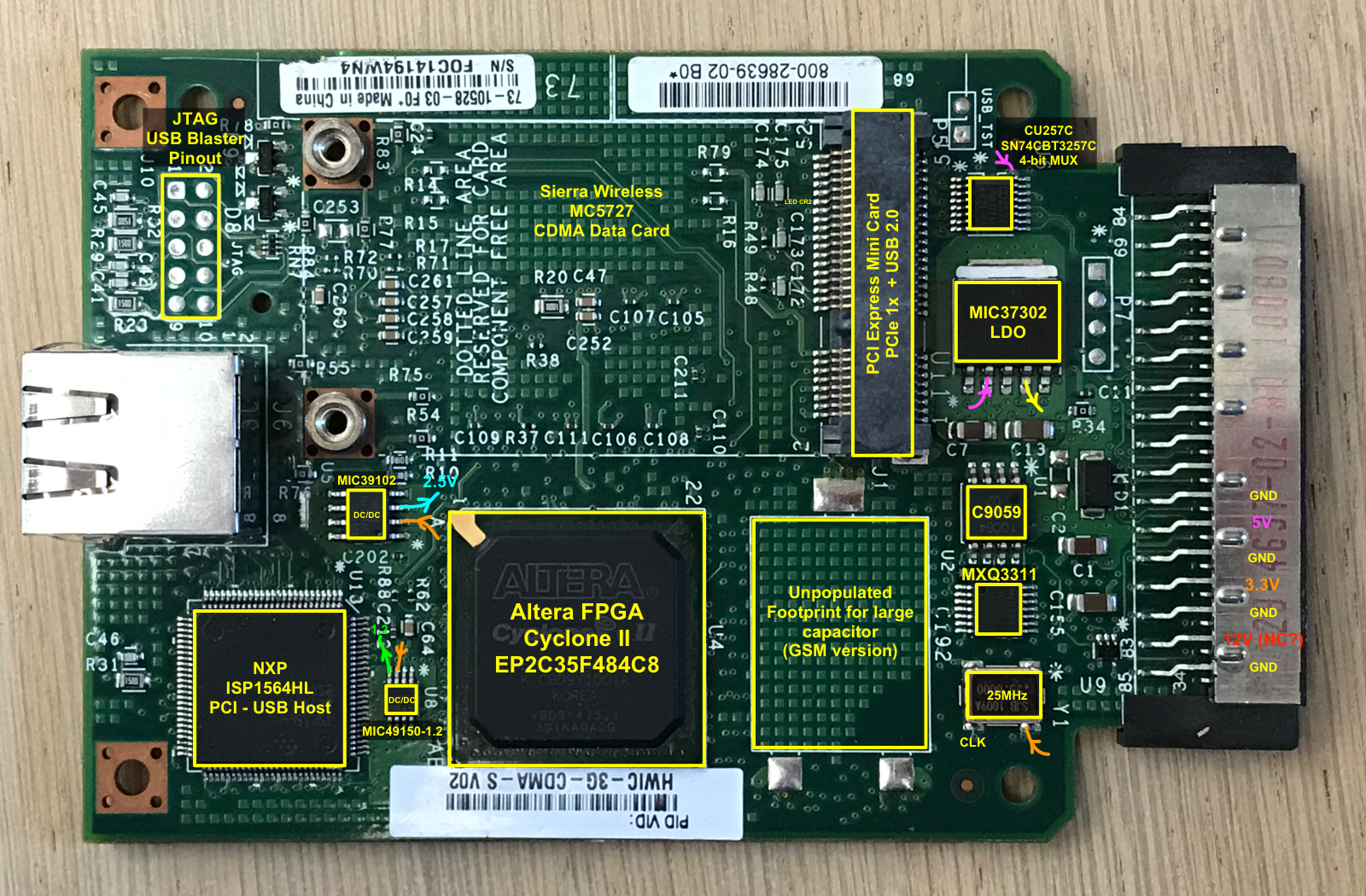
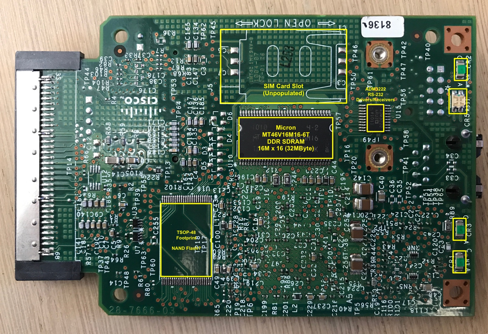
The PCB has a number of unpopulated component sites. That’s because the design is used not only for the CDMA version, but also GSM and HSPA variants, called, unsurprisingly, HWIC-3G-GSM and HWIC-3G-HSPA, both of which go for a considerably higher price on eBay.
The GSM version has a standard full-size slot for a SIM card as well as a large capacitance that’s lacking on the CDMA version.
On the back side of the PCB, there is a TSOP-48 footprint that isn’t populated for both versions. The connections between the solder pads and the FPGA are the right ones for NOR flash with a size up to 2Mx16-bit. It is possible to upgrade this board with NOR 4MByte of flash!
The core functionality of this board comes from an integrated Sierra Wireless module that slots into a PCI Express Mini Card.
Note: the wireless module is held onto the board by 2 screws that were very tight, but used a weak metal. Both screws stripped when trying to remove them, and I had to use a special screw removal drill bit to get rid of them!
Other than the wireless module, there’s the Cyclone II FPGA, and an NXP ISP1564HL USB 2.0 Host PCI controller. (Yes, that’s old school PCI, not PCIe!)
This made me scramble to Google: why in the world would you need USB on a device like this?
Turns out: a PCI Express Mini Card has support for 2 communication protocols between host and card: either PCIe 1x or USB 2.0. The more you know! Since this is custom solution designed specifically for the Sierra Wireless module, the Cisco engineers rightfully didn’t bother to wire up the PCIe interface signals.
Also present: a 32MB DDR SDRAM for all your volatile data storage needs (yay!), and the usual supporting cast of voltage controllers, level shifters, LEDs, connectors, and various unknowns.
Powering Up the Board
The first step of reverse engineering the VWIC3-2MFT-T1/E1 card consisted of unraveling its power supply architecture. That board uses the full spectrum of available power sources of the HWIC connector: 12V, 5V and 3.3V (though you cheat your way out with only a single 5V source.)
How did I figure out which pins carried which voltage? By plugging the card into a real Cisco router, of course! Not too long ago, this one cost ~$10k, but now they go for $60 on eBay.
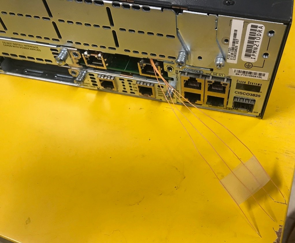
A similar exercise on this board had the following outcome:
- 12V: unused
- 5V: used to power the PCI Express card + the mystery C9059 chip
- 3.3V: used for everything else
The PCI Express Mini Card specification requires a 1.5V supply on the connector pins, but since these aren’t used by the wireless module either, they have been omitted as well.
At this stage, I was interested in getting the FPGA to talk: could I make it work by supplying only power to the 3.3V rail? I was about to find out!
But first, you need to connect to the JTAG port.
JTAG Connector
JTAG is the life blood of any reverse engineer, and thus one first things to get up and running. Some boards have a proprietary connector, some have the JTAG signals accessible as test points to which wire can easily be soldered, some don’t have anything at all.
And then there this board: it has 10 holes in 2x5 configuration with “JTAG” printed right next to it on the silk screen. Could it be that the Cisco engineers smiled up us and decided to add a standard Intel USB Blaster connector for our benefit?
A few minutes of Ohm-ing out, and the best case scenario was confirmed. Time to bring out the solder iron and desoldering needles, and install a 5x2 pin Dupont connector.
And Life There Was!
All that remained was:
- Connect the 3.3V pin to my bench power supply
- Plug in a USB Blaster to the JTAG connector
- Fire up Quartus Programmer -> Auto Scan
- Boom! FPGA detected!
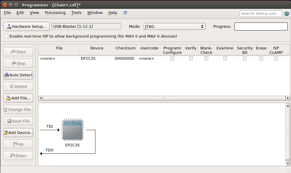
LED Blinky
The FPGA Board Hack project already figured out the connections between the LEDs and the FPGA, so with JTAG up and running, getting the LEDs to blink was a matter of minutes.
Success!
The Curious Case of Component C9059
With the Hello World of FPGA reverse engineering behind me, it was time to figure out the functionality of all other components. Most of them have sufficient markings to be identified with a quick Google search, but 2 components remained a mystery:
C9059, in an 8-pin package, and MXQ3311, in a 14-pin package. Googling these 2 devices results in no usable information. This blog post puts an end to that.
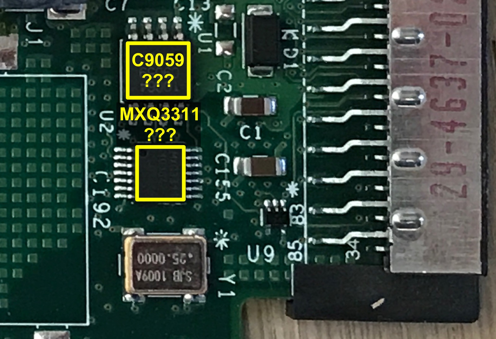
In addition to a 5V VDD and GND, C9059 has 4 pins connected straight to MXQ3311. This made me theorize that C9059 was a serial configuration PROM that contains the bitstream for the FPGA. Configured in Passive Serial mode, there would need to be some kind of microcontroller to assist with copying over the data from the PROM to the FPGA.
The earlier VWIC3-2MFT-T1/E1 card has the same C9059 chip, confirming that it provides some common functionality that is not unique to this particular design. And the Stratix II FPGA on that board has a very similar capacity in terms of logic elements, DSPs, and memories.
But while there are indeed connections between the MXQ3311 and the FPGA, these connections don’t seem to go to the FPGA configuration pins.
Even stranger, the FPGA Board Hack project also had a go at reverse engineering the VWIC3-2MFT board. When you look at the pictures of their board the C9059 and MXQ3311 footprints are not populated! Unlikely that these were desoldered after the fact, but that means that these components aren’t even essential for basic operations.
After a while (hours…) I noticed that my VWIC3-2MFT board doesn’t have an MXQ3311, but a CV9606 chip. One that doesn’t show up in any Google search either. Eventually, this made me go through all 5 of my Cisco boards to see if there were other markings to be found.
And bingo! Against all odds, the second one of my VWIC3-2MFT boards isn’t marked C9059 but 12836RCT. The top Google search hit for that results in “Secure Microcontroller for Smart Cards AT90SC12836RCT” which links to a 3 page datasheet brief:

Cisco components are expensive, but none of the key components on this board are custom silicon.
Furthermore, unlike contemporary FPGAs, the Cyclone II FPGA has no support for encrypted bitstreams or design security features where secret decryption keys can be one-time fused into the FPGA.
Without special steps, anybody could go to the open market to bulk purchase the FPGA, USB Host controller, and wireless card, clone the PCB, and sell counterfeit versions. And that’s exactly what happened in the past, as a quick search for “counterfeit Cisco” will show.
A crypto device on the board can prevent this kind of cloning: with a challenge-response authentication step, the hosting router can first verify that it is talking to a real Cisco sanctioned device before enabling the functionality of the board by downloading the required bitstream.
In a way, the full value of this product depends on a small chip that can only be purchased from Atmel by Cisco, and programmed by Cisco.
The AT90SC12836RCT has 128KB of fixed ROM and 36KB of reprogrammable ROM. Not nearly enough to contain the full bitstream (which requires 857,332 bytes), which kills the theory that these devices are used for configuration.
This leaves us with the MXQ3311/CV9606: it’s almost certainly a level shifter to translate the HWIC 3.3V levels to the 5V of the crypto chip and back.
Speaking of 5V: the datasheet brief of the AT90SC12836RCT mentions an operating range from 2.7V all the way to 5.5V. Why run the crypto chip at 5V when 3.3V would suffice?
Bitstream Configuration
With all other components identified, none of which containing flash, the only remaining option was that this FPGA gets configured by the main router at bootup.
Figuring out the HWIC pins that are reserved for this took much longer than expected: there are no straight connections between the FPGA and HWIC connector. One of the most time consuming parts of reverse engineering a PCB is tracking down connections that have one or more small passive or active component in between them. The PCB has hundreds or even thousands of them and the hidden layers on the PCB (especially on a sturdy high-quality one like this) leave random guessing as the only option.
In the end, it came all down to 3 tiny components in an SOT23-5 package, marked in red below:
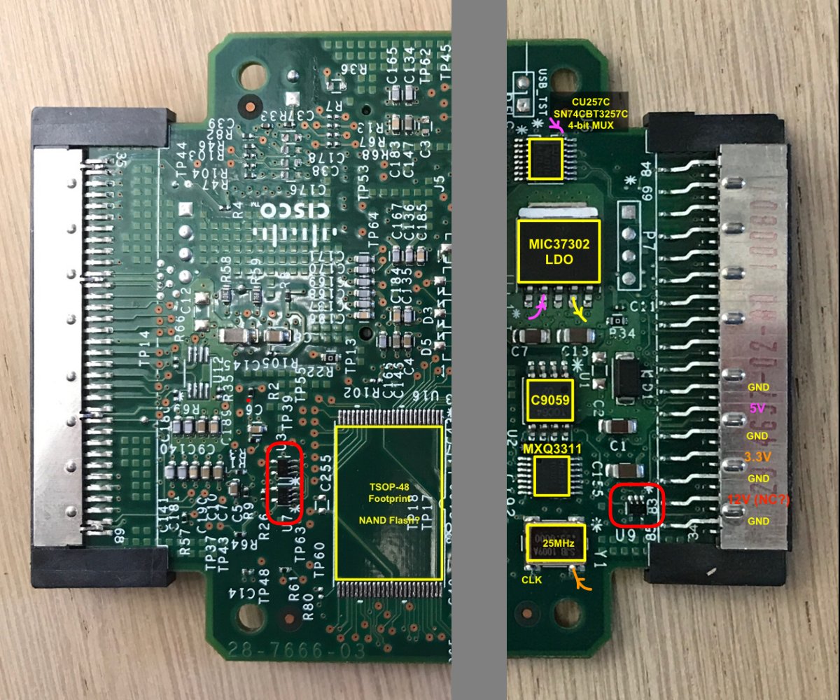
(Note: the section below was rewritten. Thanks to MorriganR for this info about how to identify SOT23-5 devices!)
The SOT23-5 packages have a marking on them with 2 or 3 letters. These indicate their function:
- U3: ‘VE’: AND gate
- U7: ‘AN’: Tri-state buffer with active high OE
- U9: ‘CGK’ or ‘VG’: OR gate
This give the following schematic:
I added Saleae logic analyzer to the HWIC pins of the schematic, plugged in the HWIC card in the Cisco router and recorded its whole boot sequence. The signals all make sense.
A major consequence of the lack of serial configuration PROM on this board is that it’s not self-hosting and thus can never be deployed without a supporting CPU that loads the bitstream at bootup.
One should be able to rig a system together with a cheap microcontroller (say, an STM32 Blue Pill) and an SD card or some other way to store ~1MB of data. But it’s definitely a negative.
Block Diagram: Putting It All Together
With that, all components and connections have been identified, giving us the following block diagram:
Low Level Connections
Block diagram is one thing, you need the know exactly which pin of the FPGA is connected to what.
When this article went to press, progress was as follows:
- All HWIC interface signals mapped
- FPGA configuration pins mapped
- Connections between FPGA and SDRAM mapped
- Connections between FPGA and RS232 connector mapped
- Connections between FPGA and unpopulated TSOP-48 solder pads for NOR flash mapped
To be done:
- Connections between FPGA and PCI USB Host chip.
The GitHub repo of this project is a work in progress and a living document, but all the low level details can be found there, and updated as soon as new information is uncovered.
(*) Hang on! This is still a developing story!