Solderless PCB Assembly with Z-tape - It's not that You Should, but Maybe You Could?
Executive Summary: in keeping with Betteridge’s Law of Headlines, it didn’t work…
- What is Z-tape?
- The Experiment
- Z-Tape Application and NOR Flash Installation
- Z-Tape Particles Up Close
- The Result
- Second Try
- Conclusion
- Epilogue
What is Z-tape?
During the “Prototyping Malicious Hardware on the Cheap” workshop at the Hackaday Superconference, Joe Fitzpatrick taught us about the existence of Z-tape. Or as 3M calls it: Electrically Conductive Adhesive Transfer Tape 9703.
Z-tape is like your garden variety double-sized tape to glue surfaces together, but with a twist: it conducts electricity, but the current can only flow through tape (the Z axis), not laterally.
The 3M datasheet explains it like this:
[Z-tape] is a pressure sensitive adhesive (PSA) transfer tape with anisotropic electrical conductivity. The PSA matrix is filled with conductive particles which allow interconnection between substrates through the adhesive thickness (the “Z-axis”) but are spaced far enough apart for the product to be electrically insulating in the plane of the adhesive.
With Z-tape, you can join together flat surfaces and create an electrical connection as well.
Z-tape sees heavy use in LCD panels where flex cables are glued straight onto the glass without needing a connector.
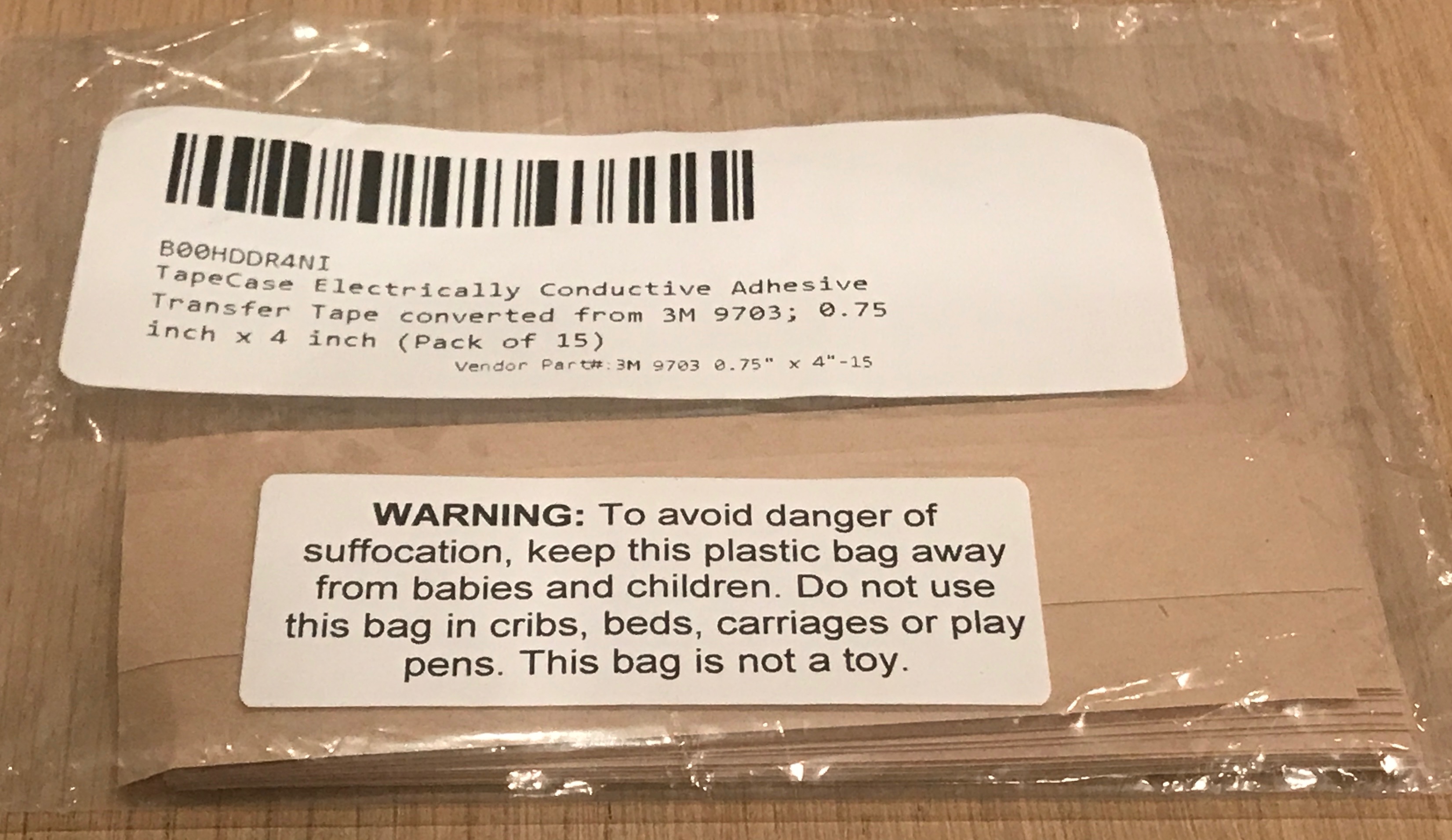
While it has seen some use in the hobby electronics circuit to glue LEDs onto copper strips, it’s not very popular due to its high cost. Adafruit charges a $5 for a 5cm by 15cm sheet. Amazon is slightly cheaper. Eager to try out it out just for the sake of it, I spent $5 for 15 4” by 0.75” sheets.
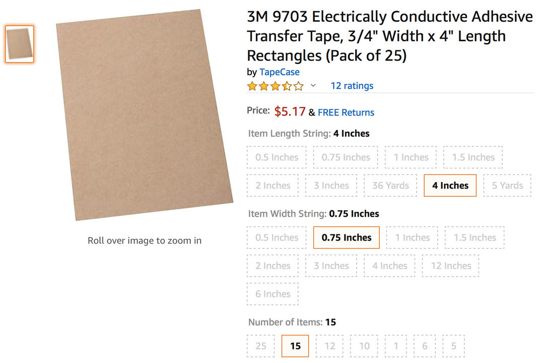
The next day, this arrived at my front door:
The Experiment
With my proverbial hammer in hand, the search was on for a suitable nail. I didn’t have to look hard to find the perfect candidate: The Cisco HWIC-3G-CDMA PCB that I just finished reverse engineering has an unused TSOP-48 footprint and connections from that footprint to the Cyclone II FPGA leave no doubt about its original purpose: a NOR flash.
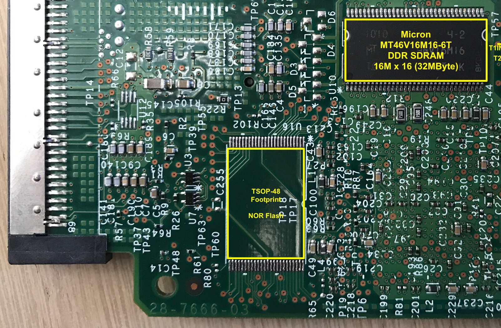
Would it be possible to upgrade this board with NOR flash without needing a soldering iron?
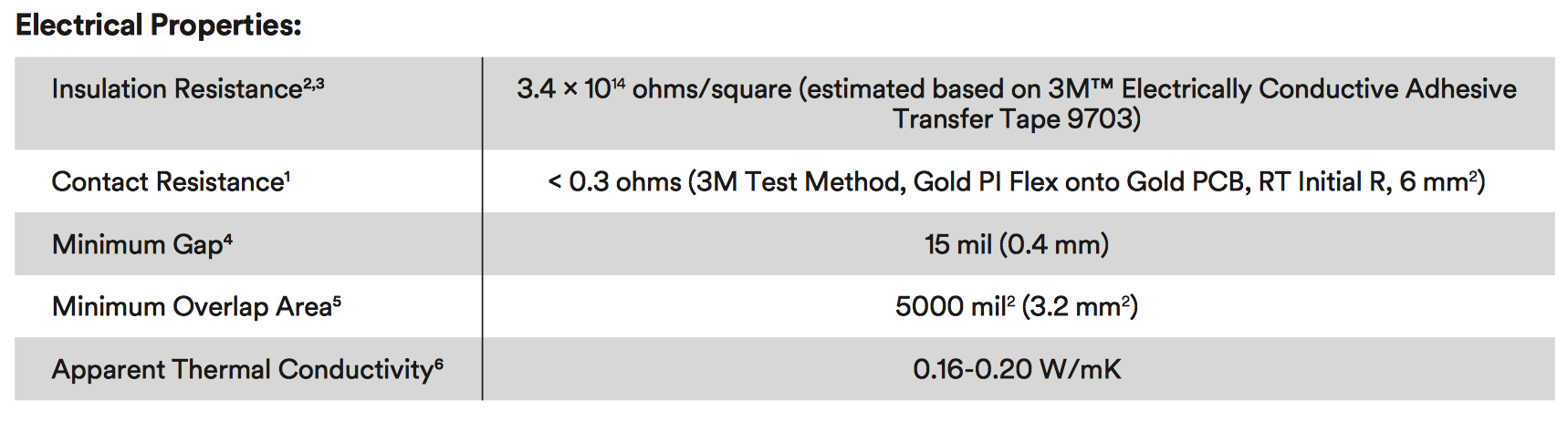
A closer look at the 3M datasheet (after the goods had already arrived, of course) reveals a minimum separation of 0.4mm between conductors. With a pin spacing of 0.5mm, we should be good on that.
But the minimum required overlap between conductors that need to be bonded together is 3.2mm2. The pins of a TSOP-48 package are just 0.5mm long and only 0.2mm wide, good for a surface area of 0.1mm2, 30 times smaller than recommended!
In addition, the flat part of these pins might not be fully horizontal, potentially reducing the chance of a good connection even more.
The odds were not in my favor, but worst case, I’d be out $5 on the tape and have to solder the NOR flash instead, like a peasant.
Z-Tape Application and NOR Flash Installation
Z-tape is an adhesive transfer tape. With regular tape like Scotch tape, the plastic strip remains after application, it’s the major factor that provides strength. The purpose of the strip of transfer tape is as a carrier of glue that helps with applying this glue in a thin, uniform layer. The strip is removed after application of the glue.
To apply Z-tape, you remove the protective layer and press the now exposed sticky part onto the surface that you want to connect (the PCB.)
After that, you need to carefully peel the other protective layer away, while making sure that you don’t rip the glue layer from the PCB. Sharp tweezers were essential to get a grip on that second protective layer.
Here you see the top row with the second layer already removed, while it’s still there for the bottom part:
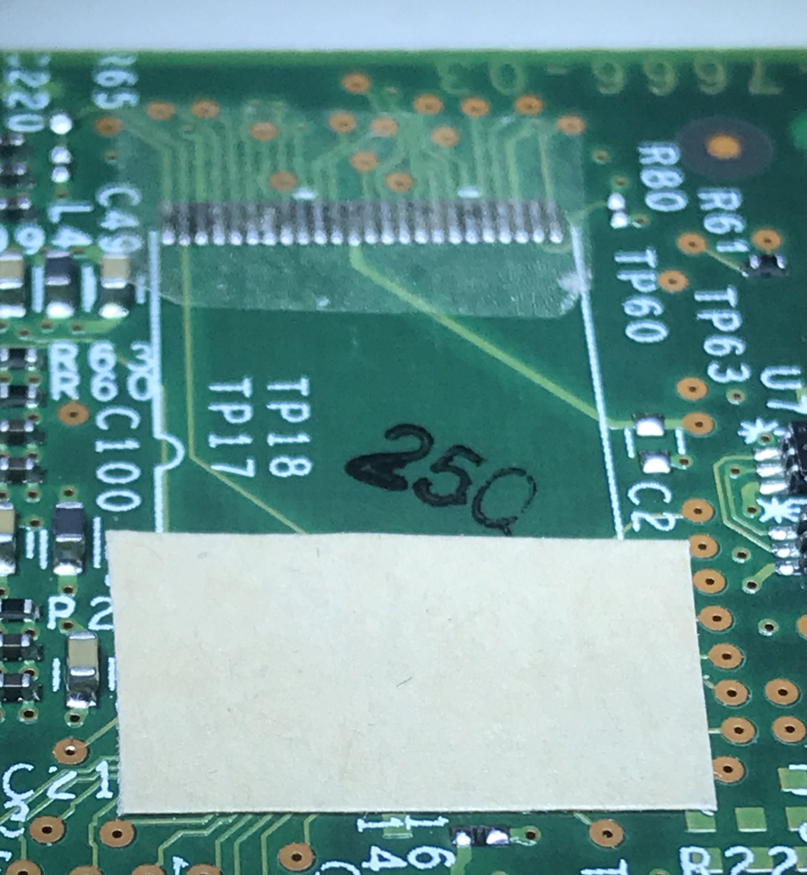
With both the protective layers removed, it’s time to install the NOR flash:
Getting all the pins of the NOR flash right on top of the solder pads was a challenge. My eyes need a microscope for this kind of precision work, but that’s too zoomed-in to have an overview of the full chip. Eventually, I was able to make it work:
After installing the flash, I squeezed on the flash to make sure there was good contact between all pins, PCB, and Z particles. You need to be careful to not push the pins off the solder pads while pressing.
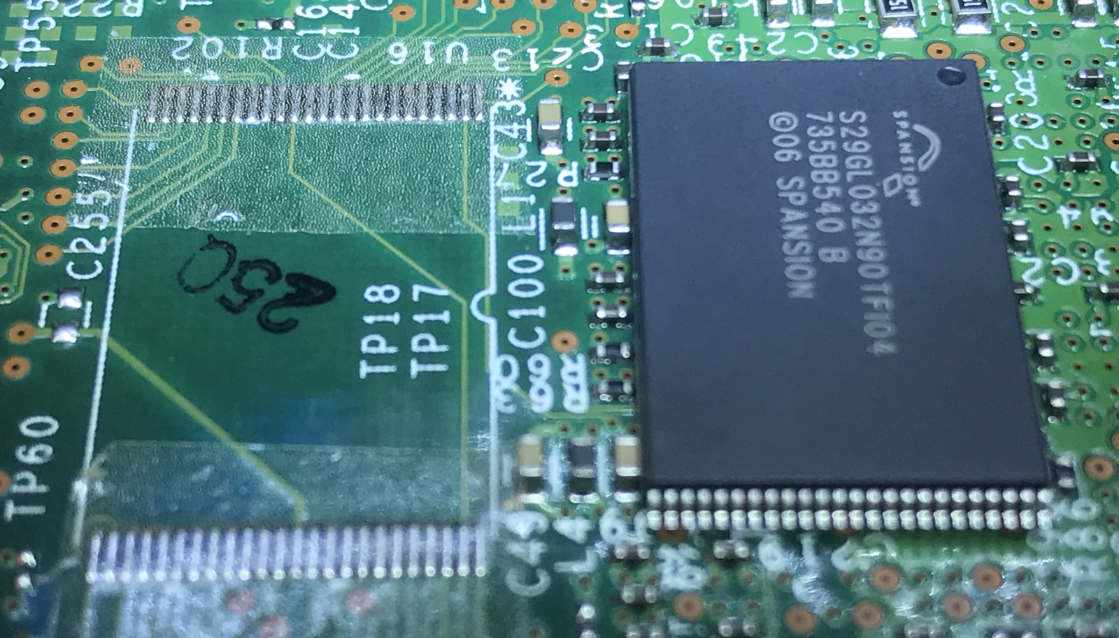
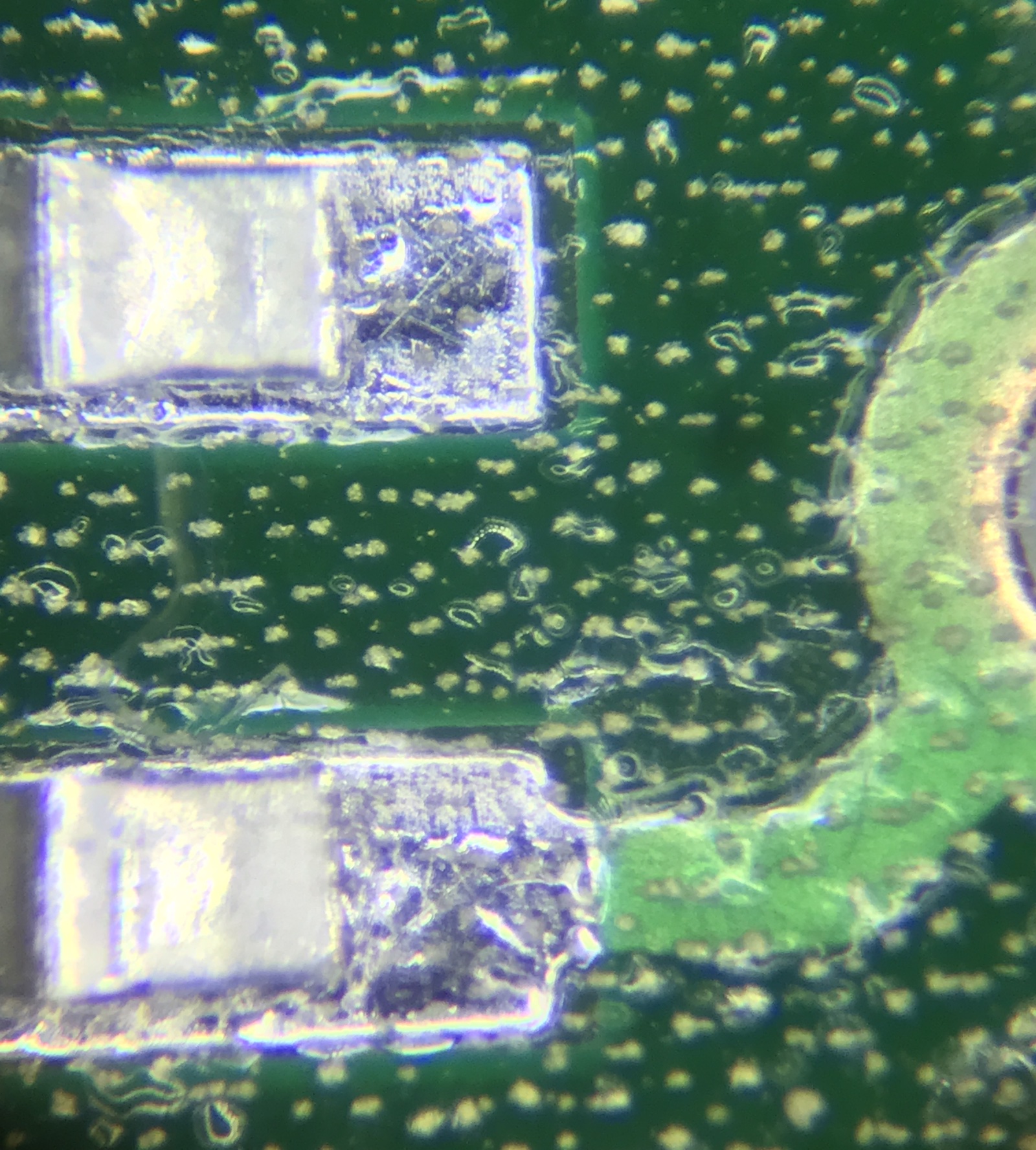
Z-Tape Particles Up Close
The NOR flash pins, spaced apart 0.5mm from each other, are a good reference to get a better idea about the size and density of the Z particles: their spacing is around 0.1mm, and their typical size about 0.05mm.
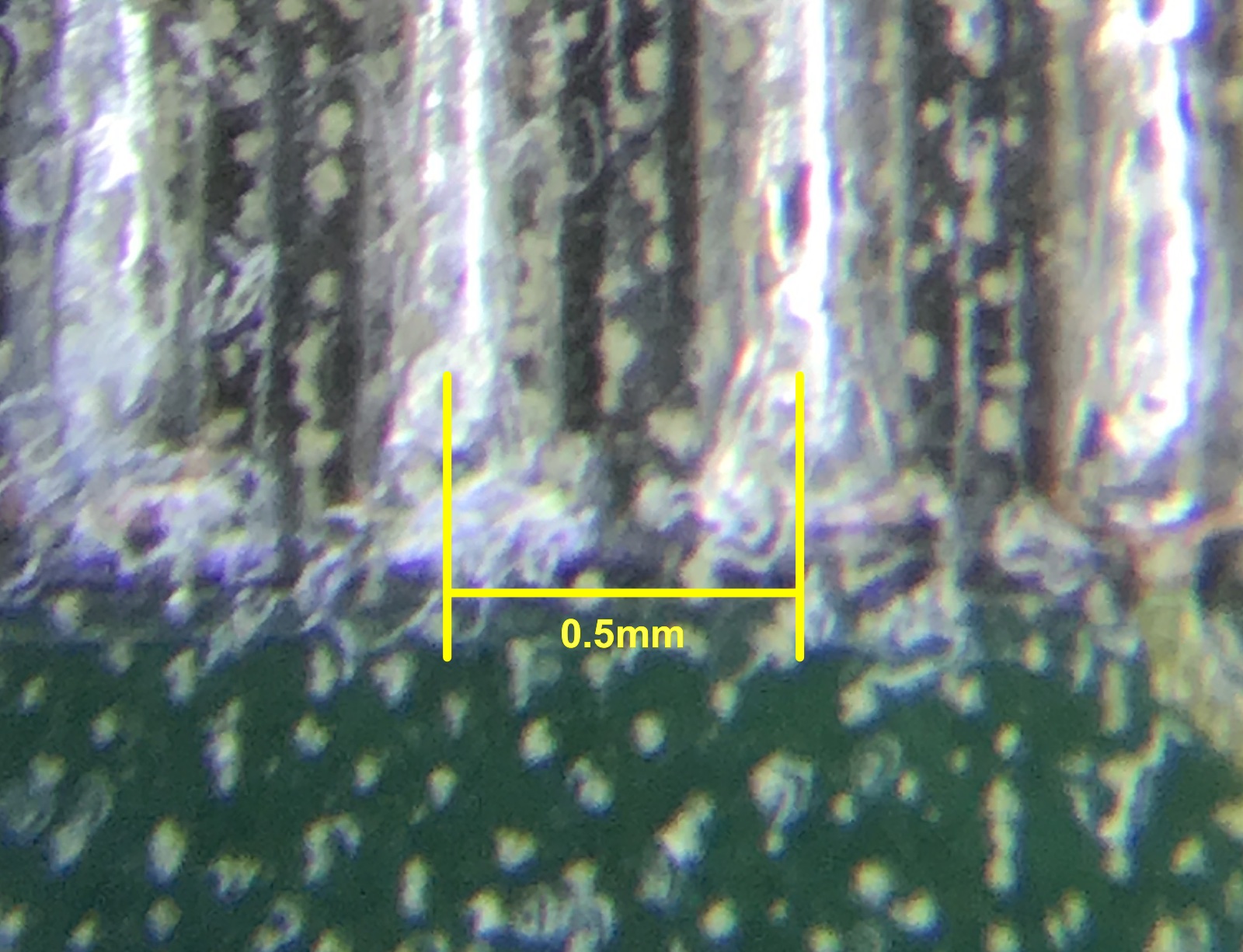
This made me somewhat hopefull about still pulling things off: it should be possible to get at least one or two grains per pin?
However, when you look at the NOR flash pins, you see how small the active area of each pin really is:
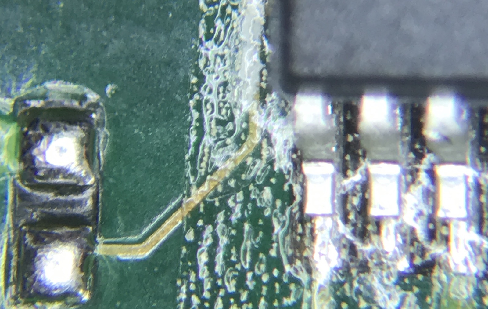
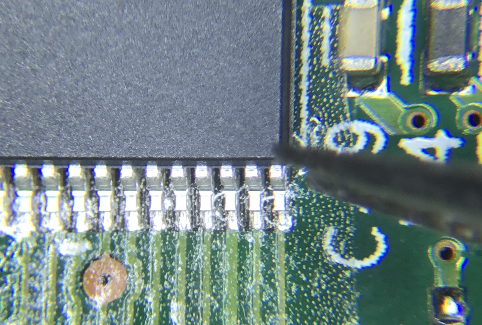
In the picture above, you see that the film isn’t very smooth anymore around the pins: that’s because I had to tear away some film to expose the testpoints needed to measure the contact between the pins and the PCB. It shouldn’t have made an impact on the part of the film that was squeezed between the pin and the solder pad. (And, indeed, there was no material difference in results between that row and the other one, which didn’t require remove part of the film.)
The Result
Time to bring out the multimeter, and check the connection between pins and PCB.
The result: not good. Terrible, in fact. Of the 48 pins, only around 5 pins made contact with the PCB.
One thing that I didn’t realize ealier was that the solder pads had solder on them, making their surface round instead of flat. With a flat-on-flat connection, the overlapping surface area was already 30 times smaller than required, these round bumps made the effective overlapping surface even smaller.
This experiment was doomed to fail right from the start…
Second Try
The pins of the NOR flash where clearly just too small to make the Z-tape experiment work. But there is a bit of statistics at work: if 48 IOs that are each 30x smaller than specified still yield a few good connections, what would happen if increase the size of the pads?
The MCP23017-SO is the I2C GPIO expander of my VGA I2C joystick board.
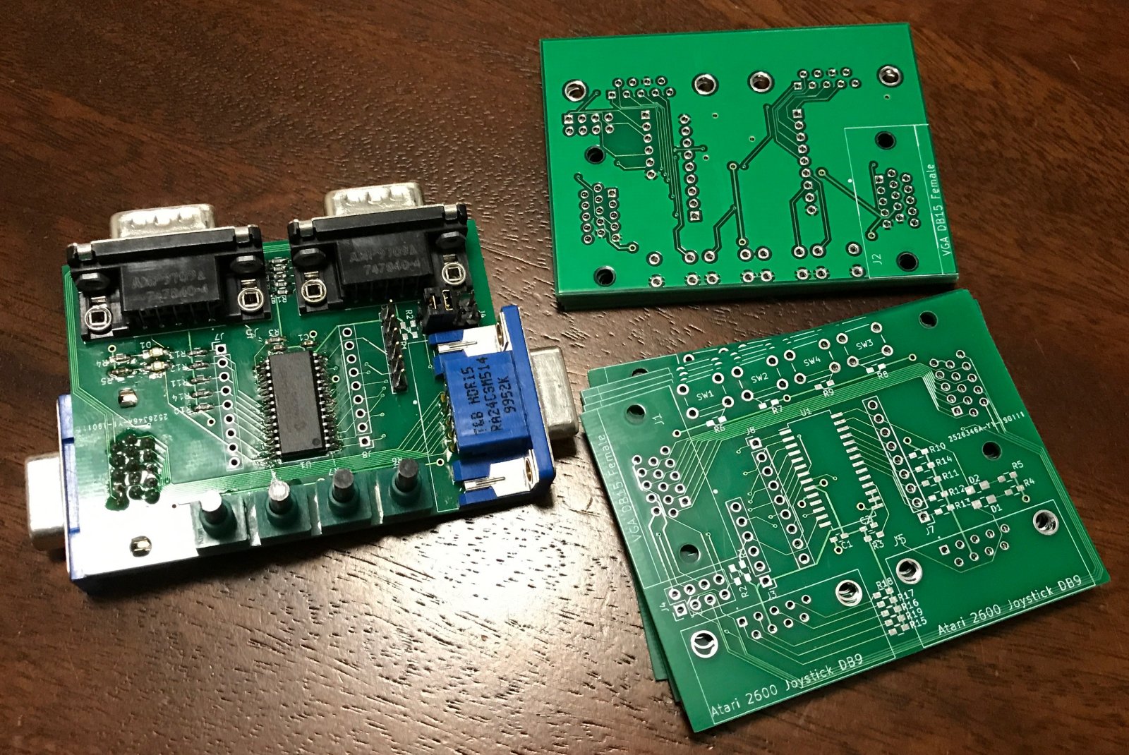
I used the version with a 28-pin SOIC package. The footprint dimensions are specified as a range, but 0.5mm x 1.00mm or 0.5mm2 is a good ballpark number, about 5 times larger than the NOR flash, though still ~6 times smaller than the minimum specification.
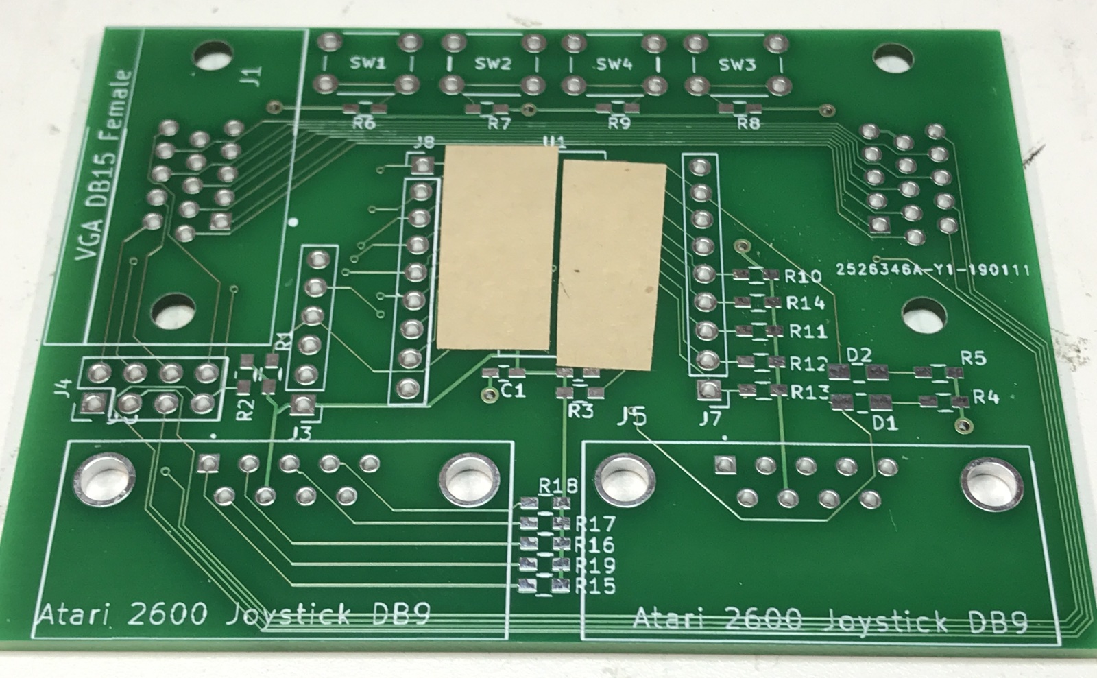
Applying the tape and mounting the chip was much easier. I pressed pretty hard to make sure the chip and the PCB both made good contact with the tape.
The results were much better: on one side of the package, all pins made good contact with the test points! But on the other side, only a few were fine. The slightest amount of pressure with my multimeter probes was sufficient to make it work, but I was never able to get things to a point where it worked reliably.
The datasheet contains these words of wisdom:
Some type of mechanical bond line compression design as determined by the end use customer (clip, clamp, screw, compressed foam, etc.) that will apply a constant minimum pressure across the bond line may be required to meet the desired end use environmental ranges and contact resistance specification.
In other words: installing a permant clamp could do wonders, but it’s kind of impractical to do when mounting chips to a PCB.
Conclusion
Z-tape is a pretty cool product. It was never intended to be used as an alternative to soldering chips onto a board and thus it doesn’t work in that capacity.
I can’t help but wonder how much the solder on the copper pads and resulting curved surface were a factor. With flat, blank copper things might have worked out better. But then you’d have to make a PCB with the specific goal of mounting a chip with Z-tape, and that was never the premise of this experiment.
I also didn’t follow all the best practices from the datasheet: I pressed hard on the chip, but maybe too hard, or not hard enough? I did not install a mechanical clamp. I didn’t heat up the glue to “improve wetting and final bond strength”.
Still, this was a fun experiment to fill a Friday evening. My remaining 14 3/4 sheets of Z-tape are going back into their bag and, for the foreseeable future, will find themselves in a warm and cozy box full of development boards, waiting to be used for some future project.
Epilogue
The NOR flash didn’t go to waste: soldering it onto the HWIC-3G-CDMA board was pretty trivial and only took a few minutes.
All I need to do now is to write some RTL to get the FPGA to talk to it!