VGA I2C Atari 2600 Joystick Expander - My First PCB
- Introduction
- The Plan
- The Process
- The Verdict
- The Redesign
- JCLPCB instead of OSH Park
- The Result
- Conclusion
Introduction
The long term goal is to be able to connect USB HID devices (mouse, keyboard, joystick) to the Pano Logic G1 and G2 units. The work on the G1 is in the very capable hands of Skip, who’s making good progress. I’ve spent some time already on the G2 but it’s slow going and sometimes you just want to work on something else.
So when Skip introduced Pano Man to the Hackaday world, it really go my attention: I wanted to run Pacman on my own G1, but I did not want to mess around with cutting VGA cables and soldering wires onto the PCB to connect a joystick.
There was a better way, one which Skip suggested in the README of his github repo:

A VGA cable has the 2 required I2C wires: they are normally used by the video source to read back an I2C EEPROM, located inside the monitor, that contains the so-called EDID: Extended Display Identification Data.
On more recent video protocols like HDMI, it’s also used to exchange data related to HDCP or to send command and status information about contrast, brightness, and a whole bunch of other parameters.
But nothing prevents us from adding an I2C slave of our own choice: a GPIO expander.
The current Pano Man implementation uses a RISC-V CPU that does nothing more than initialize the audio CODEC, after which it ingloriously goes into an endless while(1) {} loop. When using an I2C GPIO expander, it continuously bitbangs I2C transactions on the I2C bus to fetch the button status and forwards the result to the correct PacMan hardware registers. A much better use of CPU performance that would once have been sufficient to service multi-user mainframes!
The Plan
I’ve always been impressed by hobbyists like Greg Davill who are able to crank out new PCBs seemingly on a weekly basis, while never having made one myself.
This was a chance to correct that and remove a thing from the bucket list: a simple project that’s actually useful. I’d use open source KiCAD, because everybody seems to be moving to that, and have the PCB produced somewhere cheap.
The functionality was simple:
- 2 VGA connectors: input and output
- A Microchip MCP23017 I2C 16 pin GPIO expander
- 1 Atari 2600 Joystick port
- A bunch of buttons and LEDs
- 0.1” pin connectors to reuse the board as generic IO expander for other projects
How long would it take to have a PCB ready for production? Let’s see…
The Process
The GitHub repo can be found here.
- I downloaded KiCAD 5.0.1 at around 7:30pm after dinner.
- According to my GitHub logs, the first schematic was ready at 9pm.
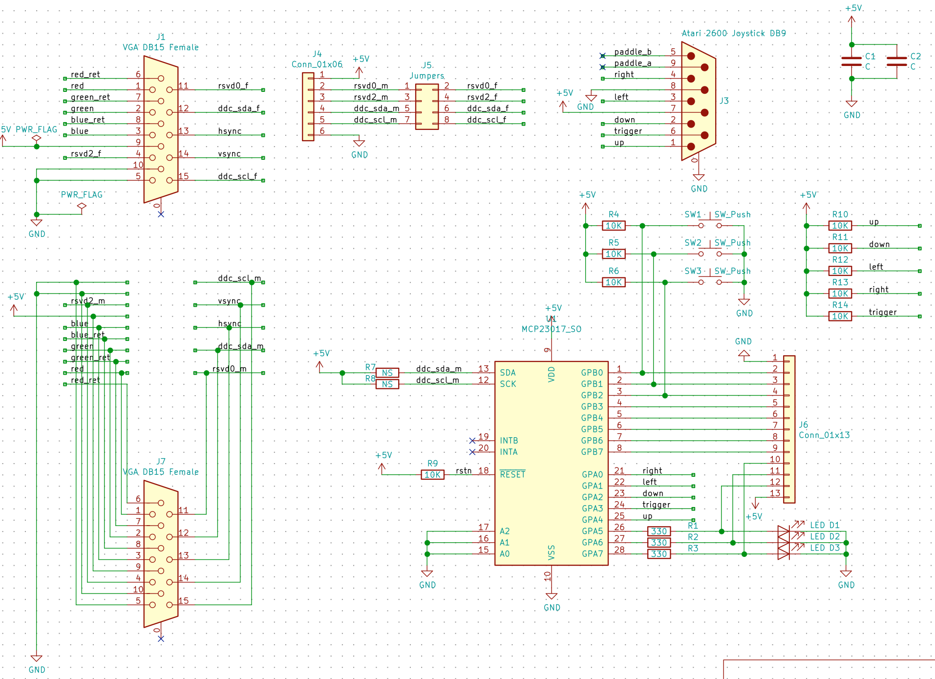
- From there, it took only 30 min to finish the PCB layout, which I could upload straight to OSH Park.
-
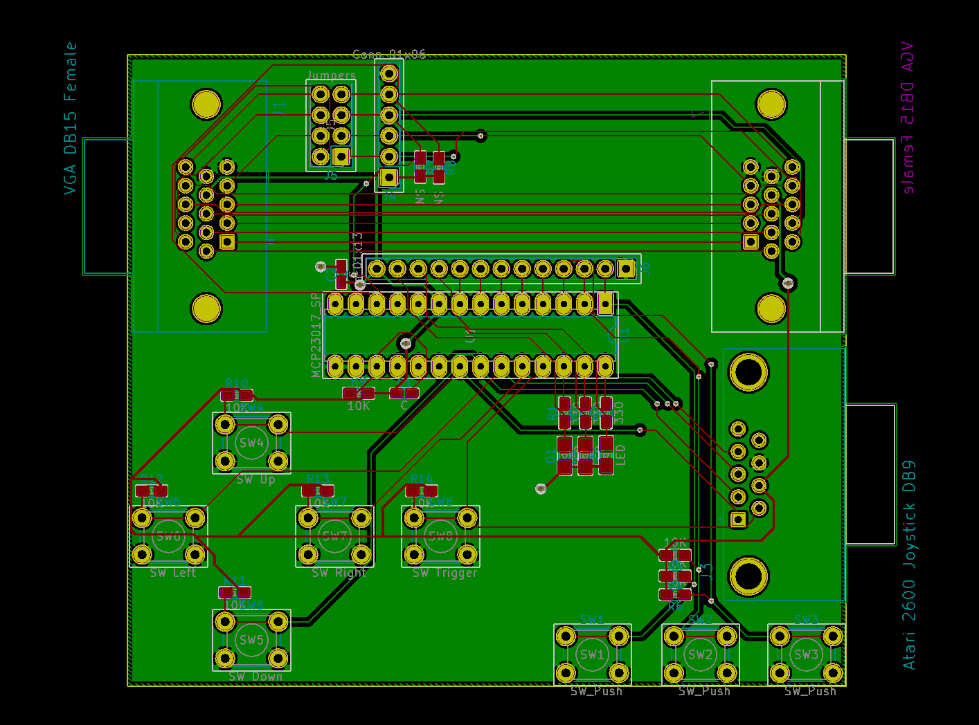
The cost was way too high ($50 for 3 PCBs), and is based on the PCB size, so I immediately redesigned the PCB and made it roughly 50% smaller.
I stripped a bunch of buttons, rearranged the connectors, switched the package of the GPIO expander from a large DIP to a smaller SMD SOIC version, and tighted the placement of the components.

-
At 11:30pm, I finished the second version, uploaded it again to OSH Park and ordered the PCBs, 3 for $27.
Much better!
After uploading a PCB layout, OSH Park will wait for other designs to come in, combine them and then produce them all at once. So even if they produce in the US, it can still take more than a week before the PCBs are ready to be shipped.
The Verdict
4 hours! 4 hours to go from downloading a complex piece of CAD software to sending out the result for manufacturing.
I found KiCAD to be an absolute pleasure to work with. A few tactical Google searches helped me get past a some hurdles here and there, but the interface is very intuitive… except for the component footprint selection which must have been designed by an alien.
The Redesign
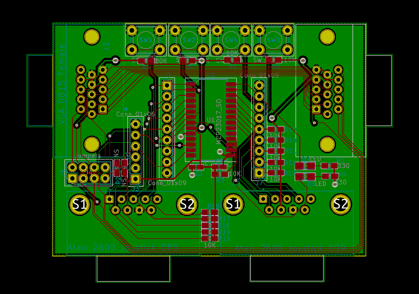
Once the design was ready, I informed Skip about my project. He immediately suggested that some games require 2 joystick ports: my little board was already more or less obsolete. Since, 2 days after the order, OSH Park hadn’t started with the production of the first board, I cancelled that one and immediately spent a second evening on a redesign:
- a second Atari 2600 joystick connector
- joystick connectors moved to a place that made more sense
- significantly tightened the routing of the VGA-to-VGA wires
- rotated the GPIO chip so that the pin connectors could be fit better
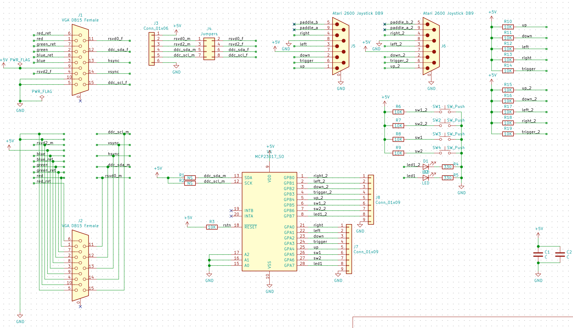
The result is slightly smaller despite adding the second joystick port! It’s certainly possible to shave some area here and there, but the board is close to the PCB equivalent of a chip being pad limited: the size of the IO ports and the buttons determine most of the dimensions.
JCLPCB instead of OSH Park
Instead of immediately uploading back to OSH Park, I wanted to see what cheap Chinese vendors could offer me. Especially JLCPCB has been very active in marketing its services by sponsoring hobbyists on Youtube.
Their offer seemed too good to be true: a $2 fixed price for 10 2-layer 10x10cm PCBs plus a $5 shipping fee.
There are a number of comments on the web about subpar quality of their products, but at just $7 there’s essentially not risk in trying.
Uploading the layout isn’t as intuitive as OSH Park because you need to create Gerber files instead of just sending the KiCAD database. But the KiCAD specific instructions are easy to follow.
Production started hours after uploading the files, on January 11th. The PCBs arrived at my doorstep on January 29th.
I don’t have much to compare to, but they looked flawless to me.
The Result
The smallest components are 0603 resistors and caps. Soldering with a regular iron was easier than I expected, but it doesn’t look as clean as it could be. That’s mostly because I had nevered soldered this small before.
For my second assembly, I’ll try solder paste and my hot air rework station.
Here it is!
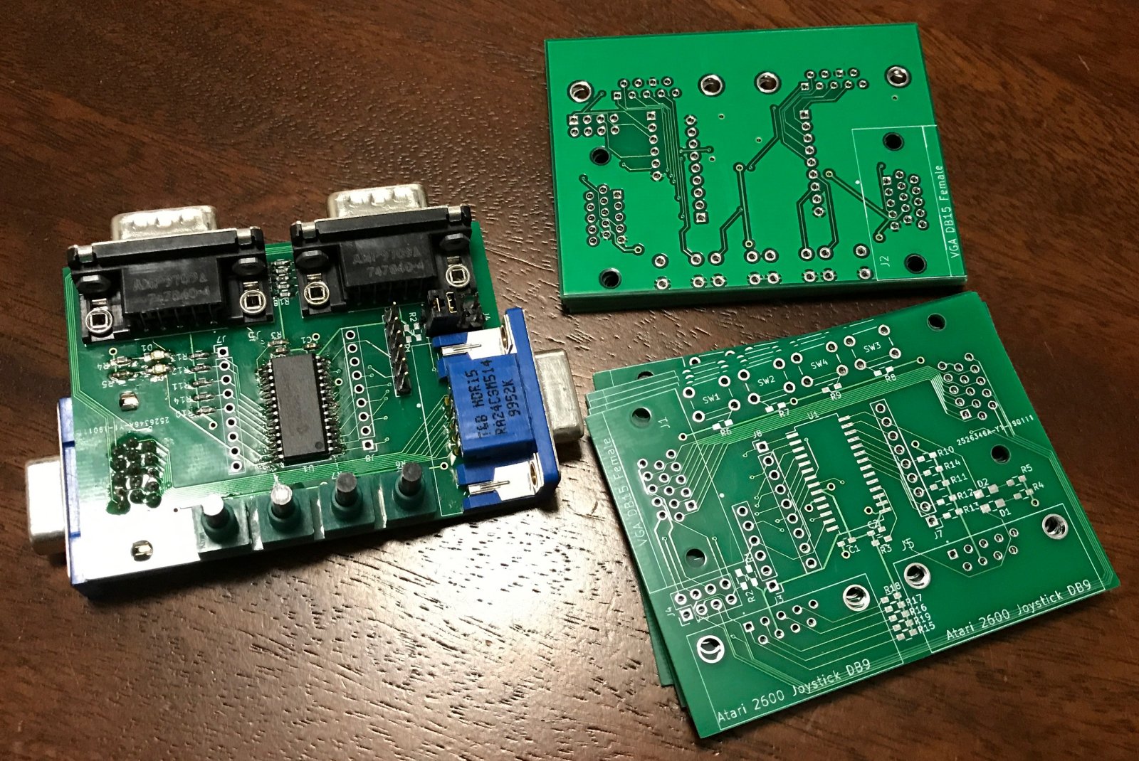
After a detour of ordering the wrong ICs (Microchip has 2 16 pin I2C GPIO expanders: the MCP23016 and MCP23017, with exactly the same package and functionality, but entirely different pinout), the board came up working right away.
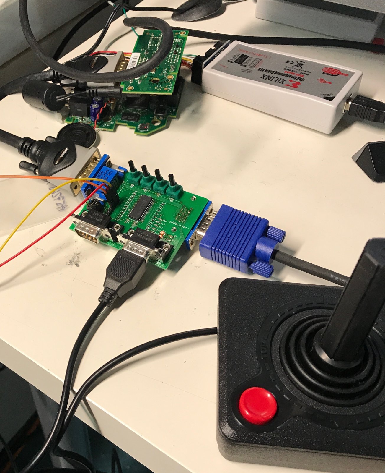
And here’s what the whole thing was all about:
The PCB isn’t perfect:
- I forgot to add mounting holes
- It’s a bit more practical and space efficient to have the VGA connectors side by side instead of on opposite ends of the PCB
- the LEDs aren’t programmed correctly just yet.
- There are 14 pullup resistors, one for each GPIO input. Those are not redundant: the GPIO expander chip has built-in pullups that can be enabled by programming a register. I can leave those empty, which will cut down on assembly time for newer boards.
- No attention was paid at all to impedance matching for the VGA wires. But I haven’t seen any adverse impact on the image quality: the frequency of the signal is probably too low to matter.
But everything is functional.
Conclusion
This project was a ton of fun! And it was way easier than I expected.
I have a bunch of more complex projects in mind. Knowing that I can just create board at low cost removes a implementation major barrier.