A Tektronix TDS 684B Oscilloscope Uses CCD Analog Memory
- Introduction
- The TDS600 Series
- The Acquisition Board
- Measuring Along the Signal Path
- A Closer Look at the Noise Issue
- Conclusion
- Fast In, Slow Out
Introduction
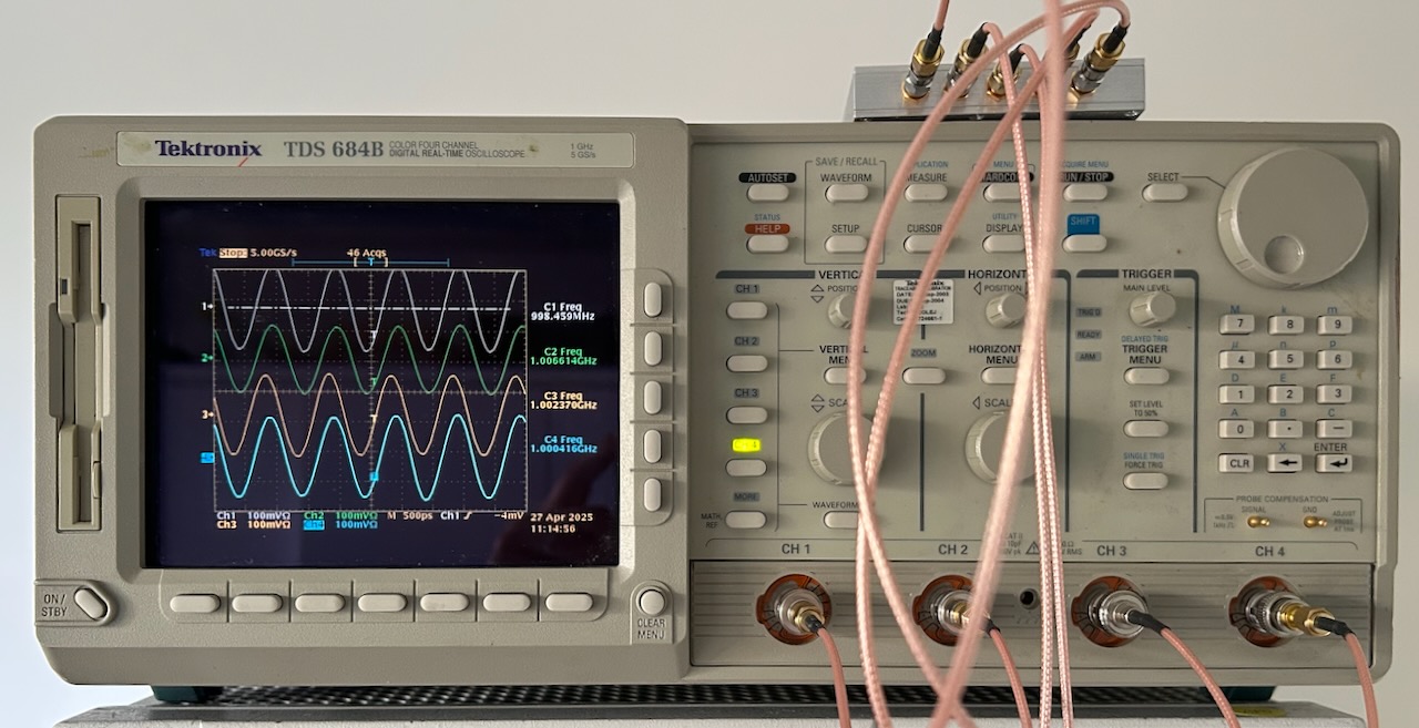
I have a Tektronix TDS 684B oscilloscope that I bought cheaply at an auction. It has 4 channels, 1 GHz of BW and a sample rate of 5 Gsps. Those are respectable numbers even by today’s standards. It’s also the main reason why I have it: compared to modern oscilloscopes, the other features aren’t nearly as impressive. It can only record 15k samples per channel at a time, for example. But at least the sample rate doesn’t go down when you increase the number of recording channels: it’s 5 Gsps even all 4 channels are enabled.
I’ve always wondered how Tektronix managed to reach such high specifications back in the nineties, so in this blog post I take a quick look at the internals, figure out how it works, and do some measurements along the signal path.
The TDS600 Series
The first oscilloscopes of the TDS600 series were introduced around 1993. The last one, the TDS694C was released in 2002. The TDS684 version was from sometime 1995. The ICs on my TDS684C have date codes from as early as the first half of 1997.
The main characteristic of these scopes was their extreme sample rate for that era, going from 2 Gsps for the TDS620, TDS640 and TDS644, 5 Gsps for the TDS654, TDS680 and TDS684, and 10 Gsps for the TDS694C which was developed under the Screamer code name.
The oscilloscopes have 2 main boards:
-
the acquisition board contains all the parts from the analog input down to the sample memory as well as some triggering logic.
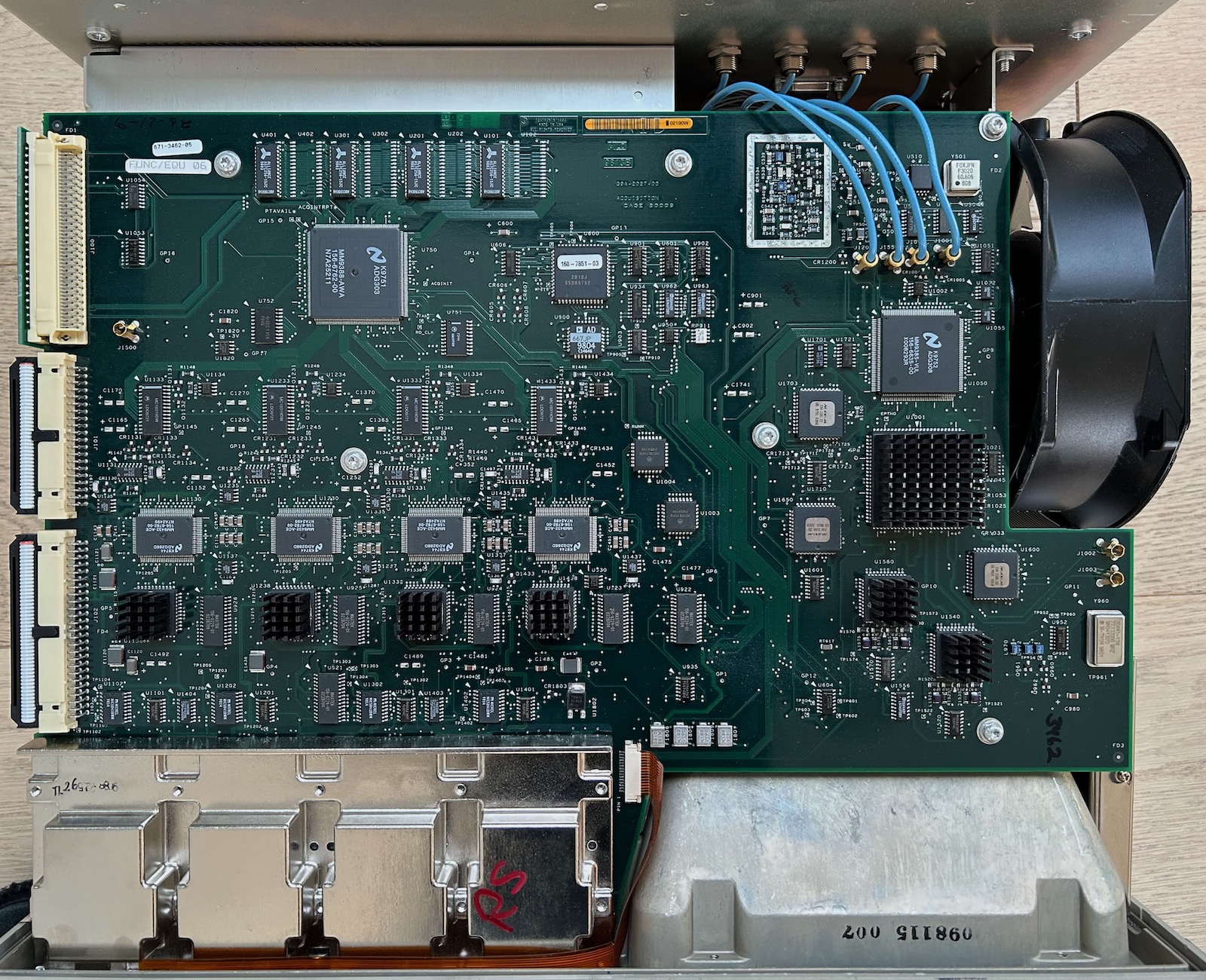 (Click to enlarge)
 -
a very busy CPU board does the rest.
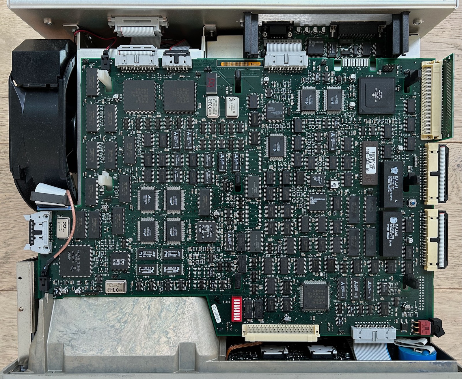 (Click to enlarge)
2 flat cables and a PCB connect the 2 boards.
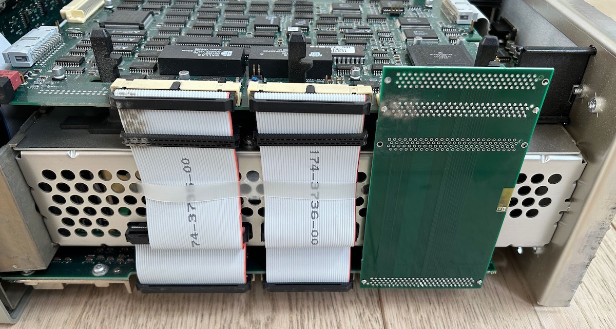
The interconnect PCB traces go to the memory on the acquisition board. It’s safe to assume that this interface is used for high-speed waveform data transfer while the flat cables are for lower speed configuration and status traffic.
If you ever remove the interconnection PCB, make sure to put it back with the same orientation. It will fit just fine when rotated 180 degrees but the scope won’t work anymore!
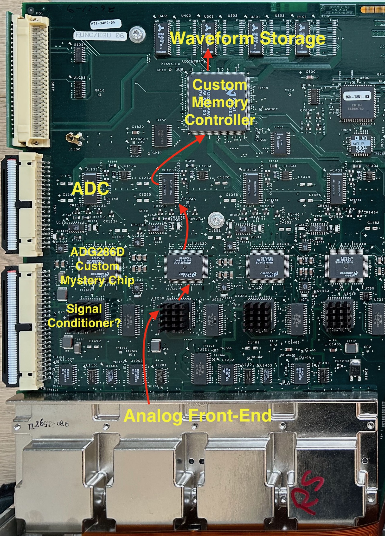
The Acquisition Board
The TDS 684B has 4 identical channels that can easily be identified.
 (Click to enlarge)
There are 6 major components in the path from input to memory:
-
Analog front-end
Hidden under a shielding cover, but you’d expect to find a bunch of relays there to switch between different configurations: AC/DC, 1Meg/50 Ohm termination, …
I didn’t open it because it requires disassembling pretty much the whole scope.
-
Signal Conditioner IC(?)
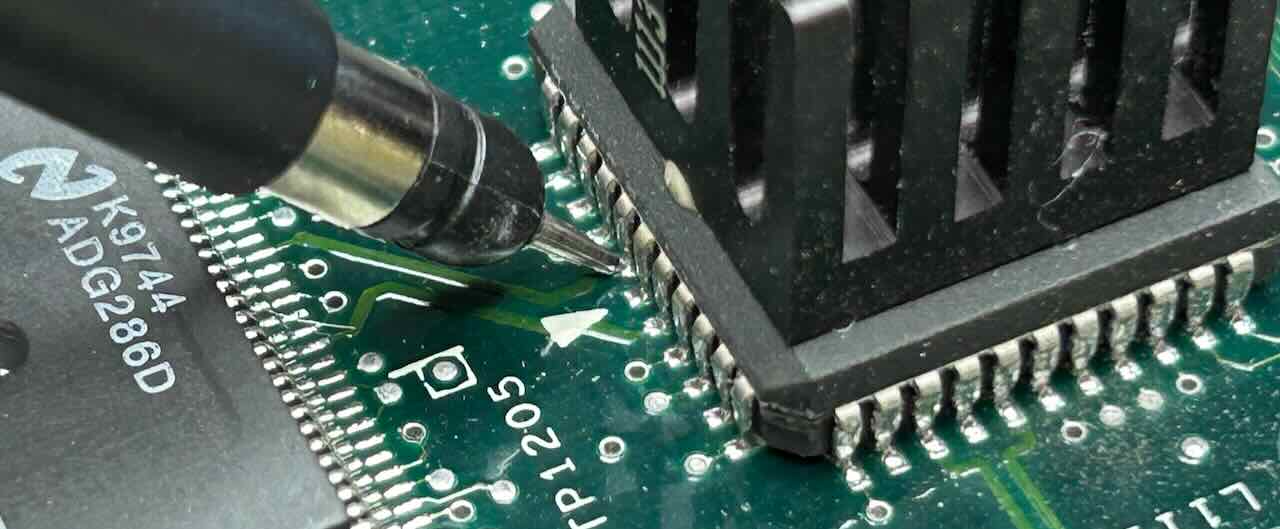
This is the device with the glued-on heatsink. I left it in place because there’s no metal attachment latch. Reattaching it would be a pain. Since the acquisition board has a bunch of custom ICs already, chances are this one is custom as well, so knowing the exact part number wouldn’t add a lot of extra info.
We can see one differential pair going from the analog front-end into this IC and a second one going from this IC to the next one, an ADG286D.
-
National Semi ADG286D Mystery Chip
Another custom chip with unknown functionality.
-
Motorola MC10319DW 8-bit 25 MHz A/D Converter
Finally, an off-the-shelf device! But why is it only rated for 25MHz?
-
National Semi ADG303 - A Custom Memory Controller Chip
It receives the four 8-bit lanes from the four ADCs on one side and connects to four SRAMs on the other.
-
4 Alliance AS7C256-15JC SRAMs
Each memory has a capacity of 32KB and a 15ns access time, which allows for a maximum clock of 66 MHz.
The TDS 684B supports waveform traces of 15k points, so they either only use half of the available capacity or they use some kind of double-buffering scheme.
There are four unpopulated memory footprints. In one of my TDS 420A blog posts, I extend the waveform memory by soldering in extra SRAM chips. I’m not aware of a TDS 684B option for additional memory, so I’m not optimistic about the ability to expand its memory. There’s also no such grayed-out option in the acquisition menu.
When googling for “ADG286D”, I got my answer when I stumbled on this comment on BlueSky which speculates that it’s an analog memory, probably some kind of CCD FIFO. Analog values are captured at a rate of up to 5 GHz and then shifted out at a much lower speed and fed into the ADC. I later found a few other comments that confirm this theory.
Measuring Along the Signal Path
Let’s verify this by measuring a few signals on the board with a different scope. The ADC input pins are large enough to attach a Tektronix logic analyzer probe:
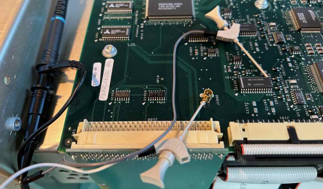
ADC sampling the signal
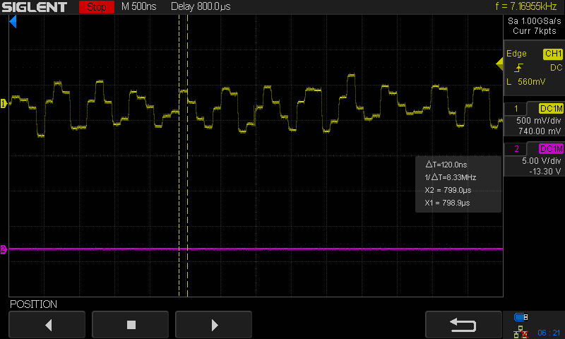
With a 1 MHz signal and using a 100Msps sample rate, the input to the ADC looks like this:
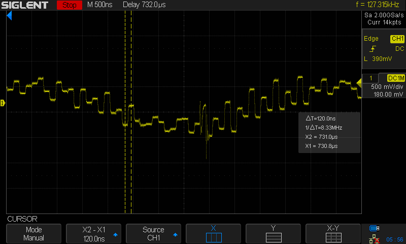
The input to the ADC is clearly chopped into discrete samples, with a new sample every 120 ns. We can discern a sine wave in the samples, but there’s a lot of noise on the signal too. Meanwhile the TDS684B CRT shows a nice and clean 1 MHz signal. I haven’t been able to figure out how that’s possible.
For some reason, simply touching the clock pin of the ADC with a 1 MOhm oscilloscope probe adds a massive amount of noise to the input signal, but it shows the clock nicely:
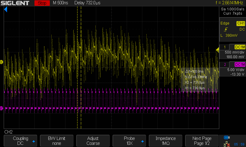
The ADC clock matches the input signal. It’s indeed 8.33 MHz.
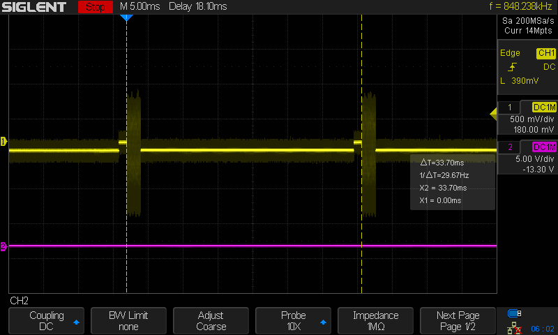
Acquistion refresh rate
The scope only records in bursts. When recording 500, 1000 or 2500 sample points at 100Msps, it records a new burst every 14ms or 70Hz.
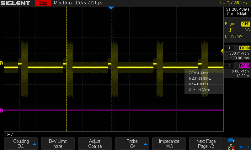
When recording 5000 points, the refresh rate drops to 53Hz. For 15000 points, it drops even lower, to 30Hz:
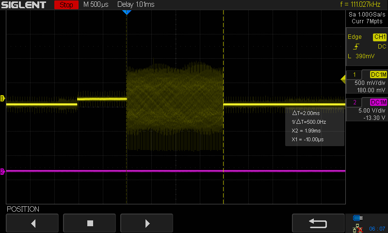
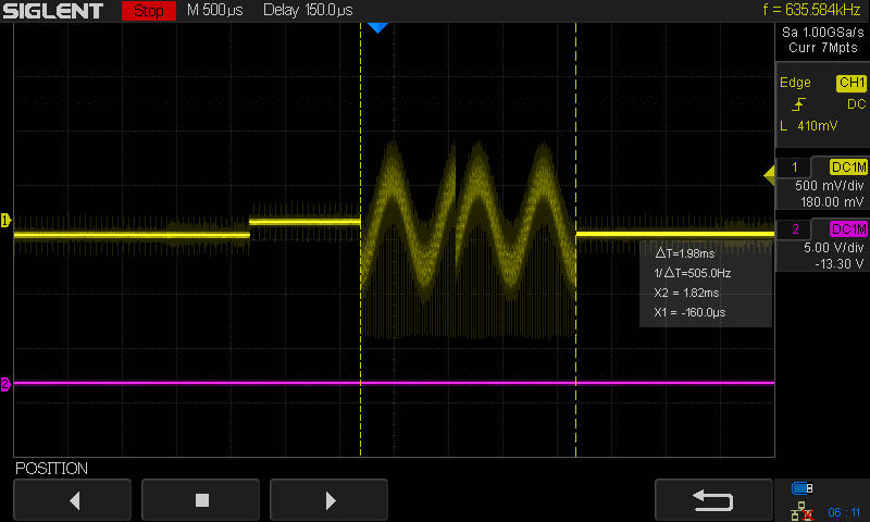
Sampling burst duration
The duration of a sampling burst is always 2 ms, irrespective of the sample rate of the oscilloscope or the number of points acquired! The combination of a 2 ms burst and 8 MHz sample clock results in 16k samples. So the scope always acquires what’s probably the full contents of the CCD FIFO and throws a large part away when a lower sample length is selected.
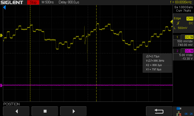
Here’s the 1 MHz signal sampled at 100 Msps:
And here’s the same signal sampled at 5 Gsps:
It looks like the signal doesn’t scan out of the CCD memory in the order it was received, hence the signal discontinuity in the middle.
Sampling a 1 GHz signal
I increased the input signal from 1 MHz to 1 GHz. Here’s the ADC input at 5 Gsps:
With a little bit of effort, you can once again imagine a sine wave in those samples. There’s periodicity of 5 samples, as one would expect for a 1 GHz to 5 Gsps ratio. The sample rate is still 8.3 MHz.
Sampling a 200 MHz signal
I also applied a 200 MHz input signal.
The period is now ~22 samples, as expected.
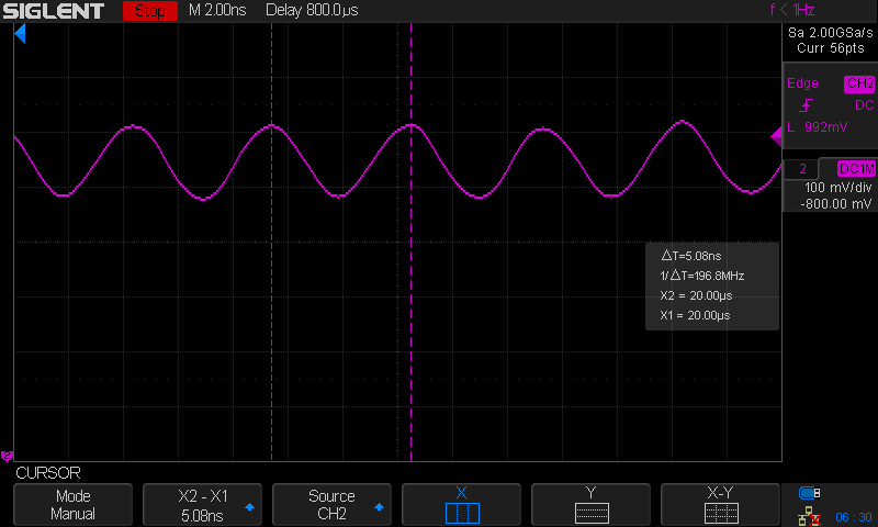
200 MHz is low enough to measure with my 350 MHz bandwidth Siglent oscilloscope. To confirm that the ADG286D chip contains the CCD memory, I measured the signal on one of the differential pins going into that chip:
And here it is, a nice 200 MHz signal:
A Closer Look at the Noise Issue
After initially publishing this blog post, I had a discussion on Discord about the noise issue which made me do a couple more measurements.
Input connected to ground
Here’s what the ADC input looks like when the input of the scope is connected to ground:
2 major observations:
- there’s a certain amount of repetitiveness to it.
- there are these major voltage spikes in between each repetition. They are very faint on the scope shot.
Let’s zoom in on that:
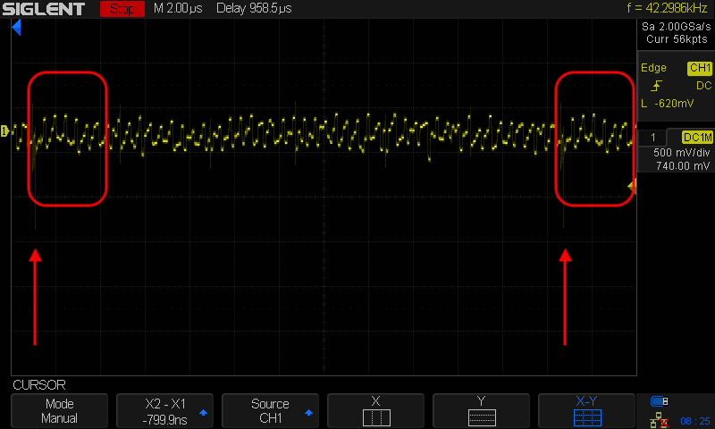
The spikes are still hard to see so I added the arrows, but look how the sample pattern repeats after each spike!
The time delay between each spike is ~23.6 us. With a sample rate of 120ns, that converts into a repetitive pattern of ~195 samples.
I don’t know why a pattern of 195 samples exists, but it’s clear that each of those 195 locations have a fixed voltage offset. If the scope measures those offsets during calibration, it can subtract them after measurement and get a clean signal out.
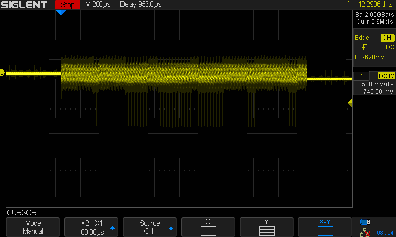
50 kHz square wave
Next I applied a 50kHz square wave to the input. This frequency was chosen so that, for the selected sample rate, a single period would cover the 15000 sampling points.
2 more observations:
- the micro-repetitiveness is still there, irrespective of the voltage offset due to the input signal. That means that subtracting the noise should be fine for different voltage inputs.
- We don’t see a clean square wave outline. It looks like there’s some kind of address interleaving going on.
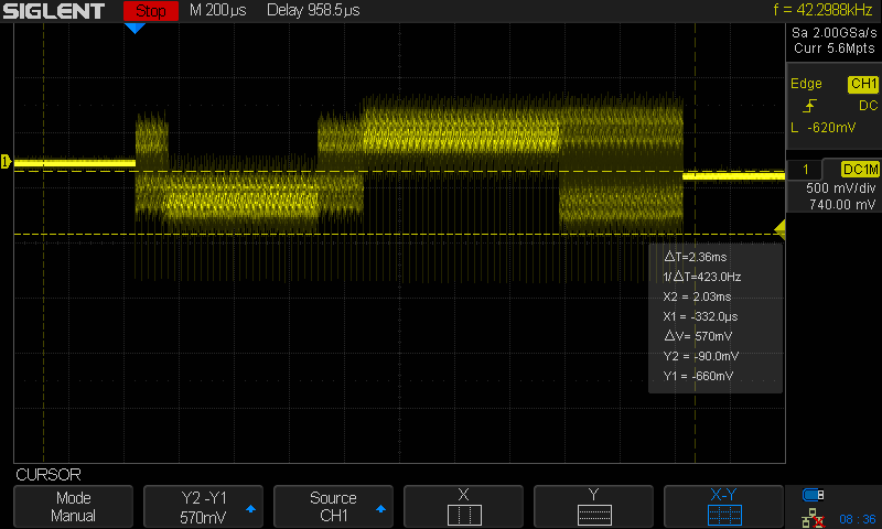
50kHz sawtooth wave
We can see the interleaving even better when applying a sawtooth wavefrom that covers one burst:
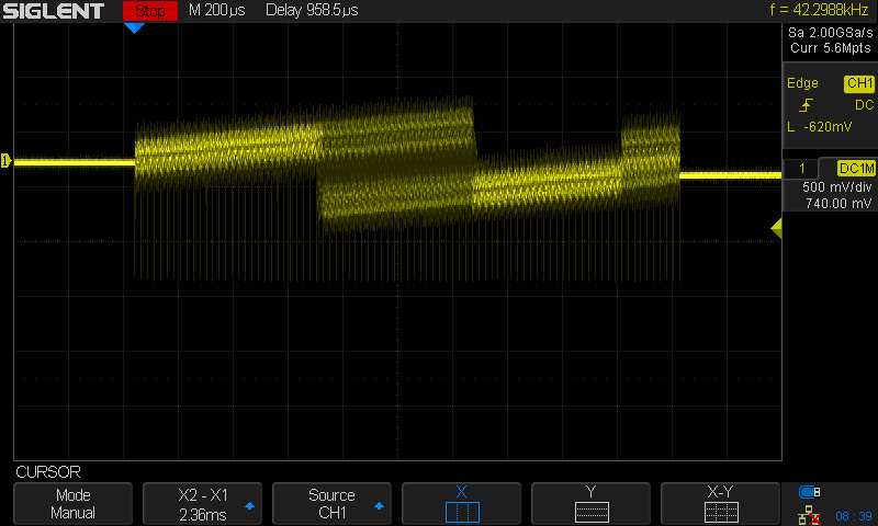
Instead of a clean break from high-to-low somewhere in the middle, there is a transition period where you get both high and low values. This confirms that some kind of interleaving is happening.
Conclusion
- The TDS684B captures input signals at high speed in an analog memory and digitizes them at 8 MHz.
- The single-ended input to the ADC is noisy yet the signal looks clean when displayed on the CRT of the scope, likely because the noise pattern is repetitive and predictable.
- In addition to noise, there’s also an interleaving pattern during the reading out of the analog FIFO contents.
- The number of samples digitized is always the same, irrespective of the settings in the horizontal acquisition menu.
(Not written by ChatGPT, I just like to use bullet points…)
Fast In, Slow Out
Through the comments on Hackaday, I learned that FISO (Fast In, Slow Out) is the magic Google search keyword for this kind of technology. Tektronix has a number of patents on it, such as US4271488A, US4648072A, US6091619A and many more. That first patent was filed in 1979. The same keyword will also trigger more search hits in various test equipment forums.