Building Multiport Memories with Block RAMs
- Introduction
- Multiple-Read, Single-Write RAMs
- Flip-Flop RAMs
- Multipumped Multi-Port RAMs
- Banked Multi-Port RAMs
- Live Value Table Multi-Port RAMs
- XOR-Based Multi-Port RAMs
- A XOR-Based Multi-Port RAM Implementation
- Which Type to Use?
- Conclusion
- References
Introduction
On-chip memories are one of the key ingredients of digital design.
In an ASIC design environment, you are typically offered a library of various configurations: single read/write port, single read/single write ports, sometimes dual read/write ports.
Once you go beyond that, you enter the realm of custom RAMs: whatever you need gets hand crafted by your RAM design team. An expensive proposition, so you better have a really good reason to need one!
It’s unusual to have a conceptual RAM like the one below readily available: one with 2 independent write ports and 2 independent read ports.

In FPGA land, things are even more limited: you get to use what the FPGA provides and that is that.
If we ignore RAMs that are constructed out of repurposed LUTs and registers, most FPGAs have so-called block RAMs (BRAMs) that have at least a single read and a single, separate, write port. FPGAs from Intel and Xilinx usually have 2 full read/write ports, but the Lattice iCE40 family, popular in the open source world, only has one read and one write port.
Unfortunately, not all design problems can map to the standard BRAMs of the FPGA of your choice.
The register file of a simple CPU will almost certainly require at least 2 read ports and 1 write port, a number that increases for multiple issue CPU architectures. And all those ports need to be serviced at the same time.
In this blog post, I go over the some common ways in which multiple read and write port memories can be constructed out of standard BRAMs. I then describe a really interesting way in which they can be designed without any major restrictions other than the number of BRAMs in your FPGA.
All RAMs will have the following behavior:
- synchronous reads only: a read operation will return the result one clock cycle later
- single direction ports only: most of the techniques discussed here can be expanded to bidirectional ports as well, but it would expand the scope of this post too much.
- reads and writes to the same address during the same clock cycle return the newly written value
- multiple writes through different ports to the same address result in undefined behavior, even if the same value is written on both ports.
Translated to an example waveform:

This blog post is heavily based on the Composing Multi-Ported Memories on FPGAs paper by Eric LaForest, Zimo Li, Tristan O’Rourke, Ming G. Liu, and J. Gregory Steffan. Images from this paper have been used with permission of the author. Eric’s website has a whole section dedicated to just this topic!
Multiple-Read, Single-Write RAMs
Register files or RAMs with multiple read ports and only a single write port are very common in small CPUs that can only retire one instruction per second: multiple read ports to gather the operands for an instruction, yet you only need 1 write port to write back the result of the instruction.
The implementation on FPGA is simple: you use 1 BRAM per read port and you connect the write ports of all BRAMs together.

Coincident reads and writes to the same address can often be dealt with by the memory generator of your FPGA. For example, the Intel Stratix 10 has the Coherent Read feature.
If not, you may have to design forwarding logic yourself. In the words of the paper:
Forwarding logic bypasses a BRAM such that, if a write and a read operation access the same location during the same cycle, the read will return the new write value instead of the old stored value. To remain compatible with the expected behavior of a one-cycle read-after-write latency, we register the write addresses and data to delay them by one cycle.
The coincident read/write problem is not specific to having multiple read ports: it’s something to be aware of whenever you use dual-ported memories.
Personally, whenever I use dual-ported memories, I simply try to avoid coincident read/writes. Either by making them impossible at the architectural level, or by imposing a requirement on the user to never do such a thing. (Don’t hold it that way!)
Flip-Flop RAMs
The trivial solution to create memories with multiple read and write ports is not use any RAMs at all, and use flip-flops instead.
It’s a solution that is often used when implementing register files of CPUs that have more than one write port.
On a RISC-V CPU with 32 32-bit registers, it will cost you 1024 FFs.
For M write ports and N read ports, you’ll also need an M-to-1 multiplexer and an N-to-1 multiplexer for each storage bit. And a truckload of wiring to connect everything together!
This doesn’t have to be a problem: the SWeRV CPU has a dual-issue pipeline that can retire 2 instructions per clock cycles. And since instructions typically require 2 operands, it requires a register file with 4 read ports and 2 write ports.
This translates into 1024 FFs, 1024 2-to-1 write and 1024 4-to-1 read MUXes, yet if you look at the ASIC layout, the register file, the orange region below marked ARF, only takes about 9% of the total CPU core area.
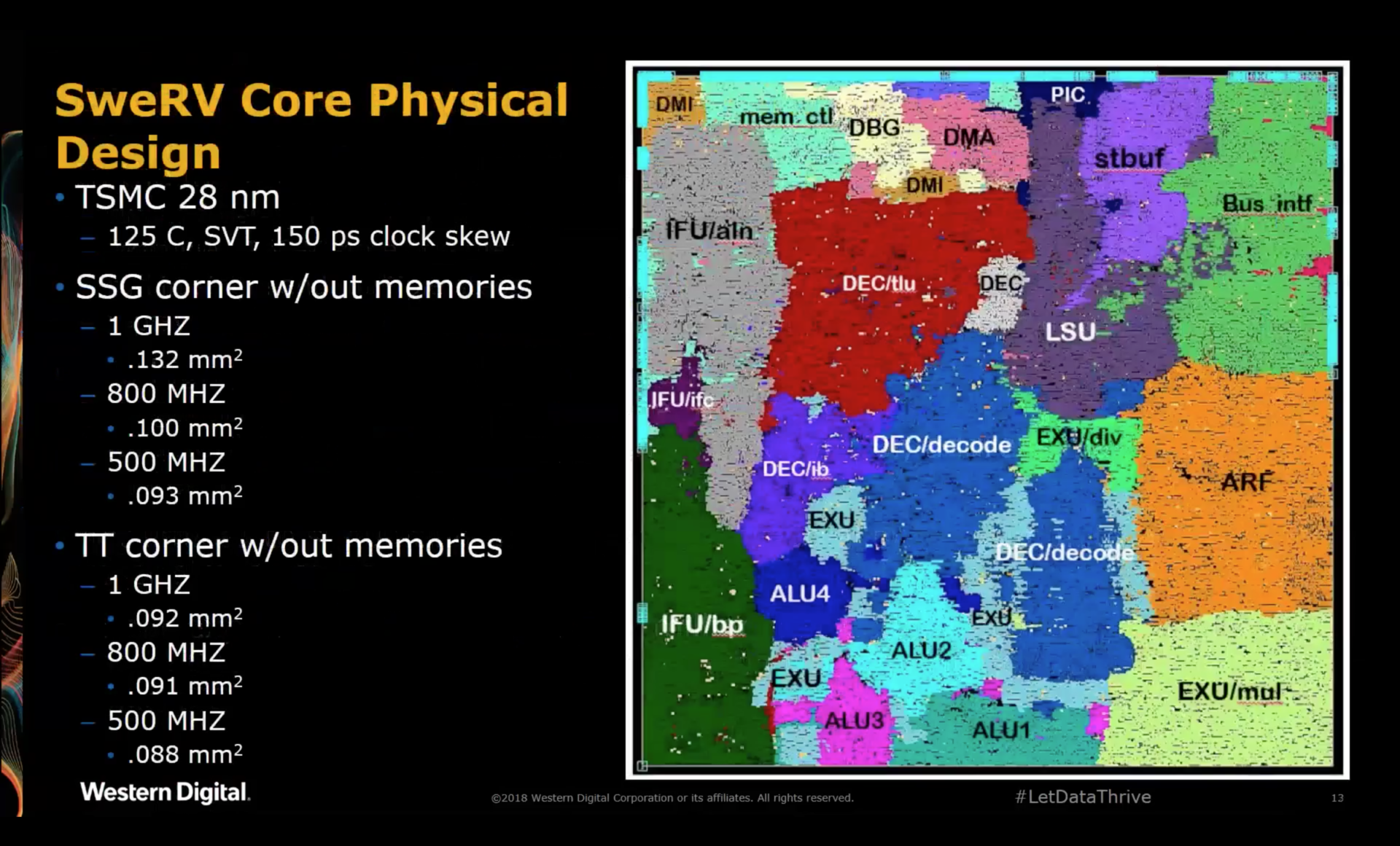
The important caveat is that the SWeRV was designed for an ASIC process, where metal layers are plentiful and a dense rats nest of wires is usually not a problem.
Translate this design to an FPGA, which often have routing wires as a constrained resource, and you’ll run into trouble very quickly! Not only will the memory be difficult to place and route, it may also quickly become a critical path of your overall design. Still, as Eric’s paper shows, for a register file of such a small size, pure FFs are usually the way to go.
Note though that 4 read and 2 write ports isn’t particularly high for a modern CPU: The 512 x 64 bits register file of the ancient Alpha 21464 CPU had 16 read and 8 write ports, with an area cost that was 5x the area of the 64KB data cache!
Multipumped Multi-Port RAMs
It’s often the case that the random logic of your design runs at a much lower clock speed than the maximum achievable block RAM clock speed of the FPGA.
You can use this to your advantage by clocking the block RAM at an integer multiple of your design, and increasing the number of read and write ports by the same integer multiple with some clever time-multiplexing.
If your design doesn’t already have such a faster clock available, you’ll also have to add a PLL to create this faster clock.
To ensure that reads and writes from and to different ports are coherent, you will need a small controller to schedule all transactions in just the right order.
But if you have spare a PLL and if your design doesn’t have to be very fast, it’s definitely a valid approach that has a good chance of being smaller than most other solutions!
Banked Multi-Port RAMs
With banking, you split one large memory into multiple smaller ones. Each memory bank stores only its fraction of the total memory.
For example, if you need 2 write ports, you could store the data for all even addresses to bank M0 and the data for all odd addresses to bank M1.
As long as you can guarantee that the 2 concurrent writes will consist of a write to an even address and a write to an odd address, you will reach a peak write bandwidth of 2 writes per clock cycle.
The problem is that this can’t always be guaranteed: 2 writes that go to the same bank will result in a so-called bank conflict, and you will be forced to serialize the 2 writes over 2 clock cycles and stall the pipeline for at least one of the write ports.
You can reduce the chance of a banking conflict by increasing the number of banks. They don’t have to equal to the number of write ports. For uniformly spread write addresses, a higher number of banks will lower the chance of a bank conflict.
The memory below has 2 write ports, 1 read port, and 4 banks. Notice how the read data output
multiplexer is controlled the 2 LSBs of rd0_addr, and how there is a signal for each write port
to stall the transaction. Not shown: the logic to decide when to stall, and which port to stall. (Though
that doesn’t have to be complicated.)

Alternatively, when the writes come in bursts with idle cycles in between, you could add a FIFO to buffer serialized writes and avoid stalls, but then you’d also need to logic to check that reads don’t fetch data that’s temporarily stored in that pending-write FIFO.
In a CPU that supports out-of-order issue, you could also try to schedule instructions such that coincident writes to the same bank are avoided as much as possible. Or you might even create an optimizing compiler that orders instructions such that banking conflicts are reduced!
Banking is not only a potential solution for multiple write ports, but for multiple read ports as well. This blog post on shared memories in Nvidia GPUs has a section on bank conflicts and how to avoid them. In fact, just google ‘bank conflict’ and you’ve find a lot of information on this topic.
Either way, things will get complex very quickly. And sometimes your design is such that stalling the pipeline is impossible, yet banking conflicts can’t be avoided.
A different solution is needed.
Live Value Table Multi-Port RAMs
The Live Value Table (LVT) approach is an extension of the technique that’s used for the single-write, multi-read RAM. Instead of using one RAM per read port, you also now have one RAM per write port. And when you have multiple read and multiple write ports, the number of RAMs is simply the multiplication of the two.
Like this:

Looks easy enough… except for the 2 red question marks! How do you know which RAM contains the last written value for a particular address? Or also: which RAM write port was last used to update a particular value?
That’s where the live value table comes in: it is itself a RAM with the same number of write and read ports, and with the same address capacity of the full RAM, but with a data width that is only as large as log2(nr_write_ports), 1 in our case with 2 write ports. It stores the number of the write port which has last issued a write to a given address. When a read is issued, the output of this extra RAM goes directly to the select input of the multipler.
How does that help us?
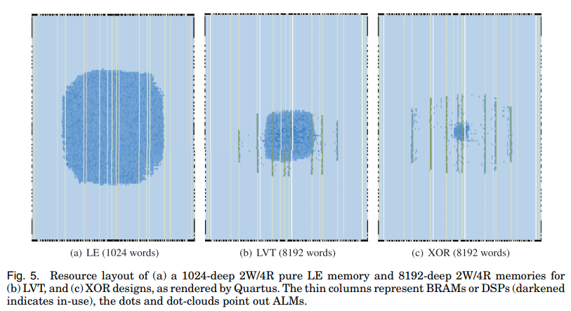
We can implement this additional multi-port RAM with discrete FFs and multiplexers only. But since the number of data bus is only 1 bit wide, the amount of logic is only a small fraction of what would be required if you’d implement the complete RAM with discrete gates!

The LVT approach is great when the size of your multi-port RAM is too large to implement with discrete gates, but primarily because the width of the data bus is too wide while the number of addresses is reasonable.
It’s also a straightforward solution that is easy to understand.
The total number of block RAMs is:
nr_block_rams = nr_write_ports * nr_read_ports
XOR-Based Multi-Port RAMs
Until now, whenever there were multiple sources from which a read port to get its data, there was multiplexer to select the correct source.
XOR-based multi-port RAMs use a different approach. They make use of the following property of the boolean XOR operation:
A xor B xor B = A
Let’s say that we have 2 registers, M1 and M2 with values OLD1 and OLD2 resp.
We update M1 with value (NEW xor OLD2).
If we now read the contents of M1 and M2 and XOR them, we get: (NEW xor OLD2) xor OLD2 = NEW.
In other words, by updating just 1 register, M1, we can recover the last written value by reading the values of both registers and XOR-ing them!
XOR-based multi-port RAMs are using this exact principle. Instead of writing the incoming value straight to the memories that are associated with a write port, we first read the values from the memories that are associated with the other write ports, we then XOR those values with the new value and only then write it.
In the diagrams below, you see how that works for a RAM with 2 write ports and 1 read port.
Unlike the LVT-base RAM, we are using block RAMs for everything. There is no storage array built out of FFs.
On the right side of the dotted vertical line, you see the RAMs that you’d also have with the LVT method. The RAMs on the left of this line are additional RAMs that are exclusive to the XOR-based method. They are the alternative to the helper RAM built out of discrete gates that contained the live value data.
Once RAMs have been written, all RAMs associated with the same write port will contain the same data.
For the sake of argument, we assume that the RAMs start out all initialized to zero. (This is not a requirement! It just makes it easier to understand.)
When you’d read the data from address 0x02, you’d get a value of 0x0000 xor 0x0000 = 0x0000.

We now write a value of 0x1111 to address 0x02 through port 0:
- first read the value from port 1 (0x0000)
- XOR that with the incoming value of 0x1111
- write the result (also 0x1111) to the RAMs of port 0:

Finally, if you now write a value of 0x2222 to address 0x02 through port 1:
- read the value from port 0 (0x1111)
- XOR it with the incoming value of 0x2222
- write the result (0x3333) to the RAMs of port 1:

You’ll notice above that if you read back the new values of address 0x02 (0x1111 and 0x3333) and XOR them, you get 0x2222, the value that was last written through port 1.
This technique can easily be expanded to more read or write ports. In the diagram below, you see the configuration for 2 write ports and 2 read ports. Just like with the LVT example, we have now 4 RAMs on the right side of the dotted line. The RAMs on the left side remain the same, but they would expand quickly if you’d increase the number of write ports.

The total number of block RAMs used by the XOR technique is:
nr_block_rams = nr_write_ports * ((nr_write_ports-1) + nr_read_ports).
The number of block RAMs goes up quickly with the number of write ports. Here we just go from 2 to 3 write ports:

An important caveat with the XOR-based approach is the fact that you first need to read a value from a RAM before you can store the new value.
If we want to retain the RAM behavior that were laid out the introduction (a read latency of 1 clock cycle and concurrent read/write resulting in the newly written value being read), then we need to add some bypass paths to make that work.
A XOR-Based Multi-Port RAM Implementation
An implementation is always useful to get a really good feel about something, so I wrote the RTL for a XOR-based RAM with 2 write ports and 1 read port.
I used SpinalHDL, which I’ve written about before, but it’s pretty trivial to port this to Verilog. Or you could use the Verilog that’s generated by my SpinalHDL project.
I assumed that there was no built-in support for concurrent read/write RAMs, which means I had to write the logic myself for the writeFirst case (that’s the case where a concurrent read/write results in the read returning the newly written data.)
The base RAM is then a simple one with 1 write port and 1 read port.
And there’s the bypass path:
        val rd_eq_wr = io.wr_addr === io.rd_addr

        val bypass_ena_p1 = RegNext(io.wr_ena && rd_eq_wr)
        val wr_data_p1    = RegNextWhen(io.wr_data, io.wr_ena && io.rd_ena && rd_eq_wr)

        io.rd_data := bypass_ena_p1 ? wr_data_p1 | rd_data_mem
The 2-write port version builds on this simple RAM.
Due to the pipelining where you first need to read before doing a write, this one also has its own bypass logic:
        val rd0_eq_wr0      = io.wr0.addr === io.rd0.addr
        val bypass0_ena_p1  = RegNext(io.wr0.ena && rd0_eq_wr0)

        val rd0_eq_wr1      = io.wr1.addr === io.rd0.addr
        val bypass1_ena_p1  = RegNext(io.wr1.ena && rd0_eq_wr1)

        io.rd0.data :=  bypass0_ena_p1 ? wr0_data_p1 |
                       (bypass1_ena_p1 ? wr1_data_p1 |
                                         bank0_rd0_xor_data_p1 ^ bank1_rd0_xor_data_p1)
You can simulate this RAM by issuing the following command:
sbt "runMain multi_port_mem.MultiPortMemSim"
Which Type to Use?
For general purpose multi-ported memories, we have now 3 different techniques:
- Discrete gates
- LVT-base RAM
- XOR-base RAM
This raises the question: which one to use for which case?
The paper on which this blog post is based goes deep into this, comparing logic gate use, RAM use, and Fmax.
In some cases, the difference can be very signficant. Here’s a case where the XOR-based implementation is clearly the best choice… if you have plenty of block RAMs to spare.
But the real answer is: it depends. Any one of the 3 methods has use cases that come out on top, depending on the data bus width, number of addresses, number of read ports, number of write ports, and desired Fmax.
Here’s just one of the graphs that compares the different implementations when using an Intel/Altera Stratix IV FPGA.
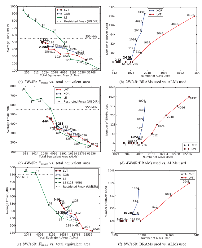
The paper contains many more tables and graphs. It even compares Altera vs Xilinx as well. It wouldn’t make sense to just copy everything. Go to the source!
Conclusion
Memories with generic multiple write ports are rarely used in digital hardware designs but maybe one day, you’ll run into a case where you absolutely need them. If you don’t have custom RAM design team to help you out, the techniques presented here may help you out.
And if, like me, you’ll never need them, I hope that you found it interesting enough to give them a closer look.
References
-
Multi-Ported Memories for FPGAs
Overview of research in this field.
-
Composing Multi-Ported Memories on FPGAs (LaForest, 2014)
Paper on which this blog post is based.