SweRV - An Annotated Deep Dive
- Introduction
- SweRV Deep Dive during Bay Area RISC-V Group Meetup
- SweRV Core Complex
- SweRV Core Microarchitecture
- SweRV Pipeline Diagram
- SweRV Core Branch Prediction and Handling
- SweRV Instruction Set Simulator
- SweRV Physical Design
- SweRV Core Performance
- RISC-V Code Density and Optimization
- Various
- SweRV for Hobby Use?
- Formal Verification
- Parting Thought about Performance
Introduction
Every 6 months, the RISC-V consortium organizes a two day workshop where various companies and research entities present work that is one way or the other related to RISC-V.
At the November 2017 workshop, storage company Western Digital announced their intention to become a major contributor to the RISC-V ecosystem and set a goal to sell more than a billion RISC-V capable CPU cores to the market every year. At the time, it was one of the first major technology companies to put their full weight behind RISC-V.
They committed to accelerating the ecosystem as follows:
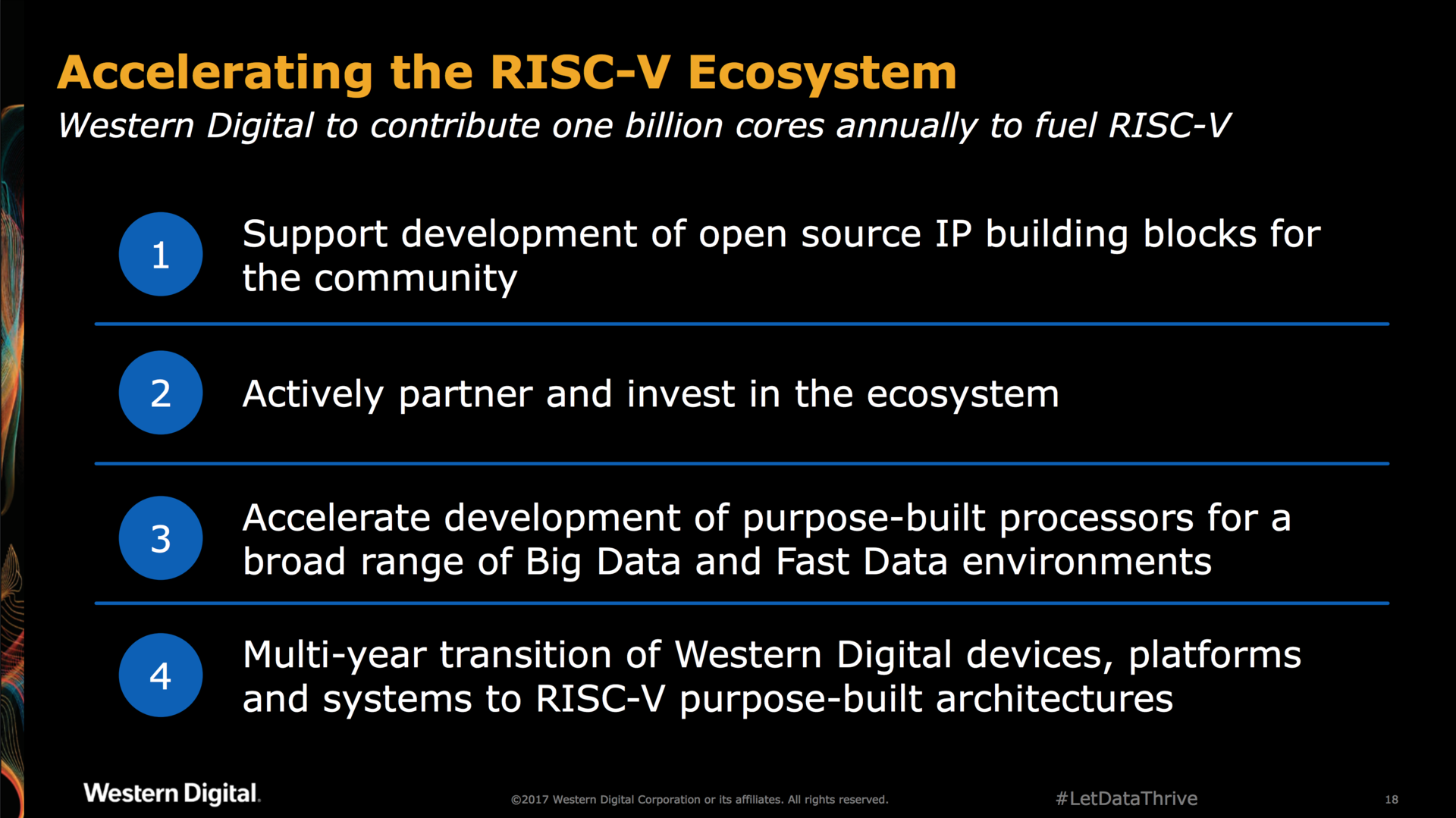
Open source IP building blocks? A promising tease indeed!
At the May 2018 workshop, the first specifics of their RISC-V IP were disclosed:
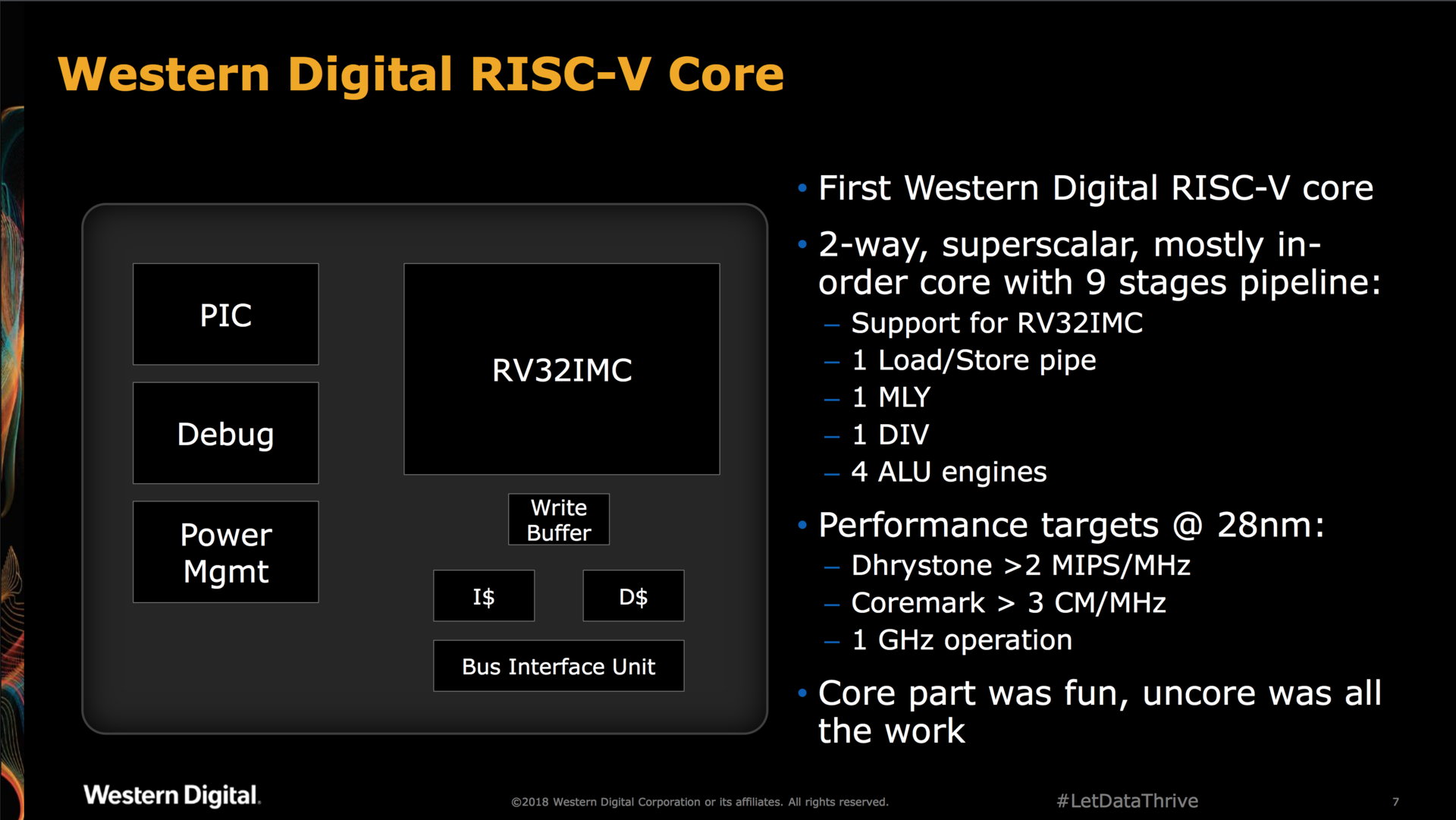
A performance of at least 3 CoreMark/MHz isn’t bad, but if the real number is close to that lower bound, it’s not stellar either when compared to, say, the Boom v2 which promises a score of 3.92 CM/MHz and 4.70 CM/MHz for resp. a dual or quad issue core:
Meanwhile, the SiFive E76 core promises 4.9 CM/MHz using a two-way superscalar in-order 8 stage pipeline.
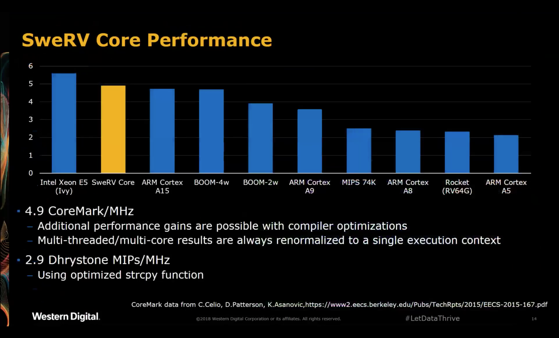
The December 2018 workshop finally saw the unveiling of Western Digital’s SweRV core, announcing an excellent 4.9 CM/MHz, just like the SiFive E76 core, with target clock speed up to 1.8GHz on an unspecified TSMC 28nm process.
Keeping their promise of a year earlier, Western Digital also announced that the core would be available as open source under the liberal Apache 2.0 open source license, with instruction set simulator (ISS) and testbenches included as well!
In a separate session at the same workshop, lower level architectural details were provided, as well as a detailed schedule of the public release of the code.
All of this culminated with the Febrary 15 release of the full source code on Western Digital’s GitHub page.
After implementing a very low performance RISC-V core myself, and after reviewing the internals of the VexRiscv, it was time to look at the other end of the RISC-V performance spectrum!
SweRV Deep Dive during Bay Area RISC-V Group Meetup
To satisfy the true geeks, Western Digital organized a Swerv Deep Dive at the Bay Area RISC-V Meetup. The meetup was well organized (free food!) and attended by roughly 100 people.
A Webex recording of this meetup is currently still available here. (The first 53 minutes are empty. The meat of the presentation starts at the 53min30 mark.)
Zvonimir Bandic, Senior Director of Next Generation Platform Technologies Department at Western Digital, gave an excellent presentation, well paced, little marketing fluff, with sufficient technical detail to pique my interest to dive deeper in the specifics of the core. I highly recommend watching the whole thing. There was also a second presentation about instruction tracing which I won’t talk about in this post.
In this blog post, I’ll go through the presentation and add some extra details that I noted down at the meetup or that were gathered while going through the SweRV source code on GitHub or while going through the RISC-V SweRV EH1 Programmer’s Reference .
The full set of slides, as copied from the WebEx stream, can be found here.
SweRV Core Complex
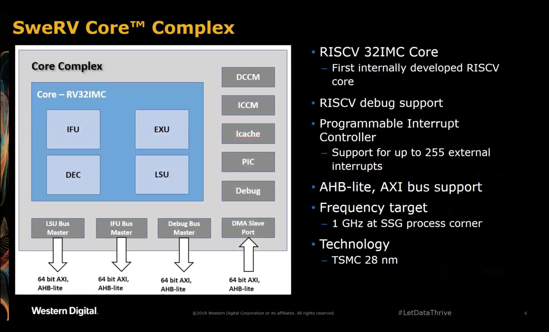
The core complex has most of the features you’d expect from a modern embedded CPU:
- the core itself
-
instruction and data closely coupled memory (ICCM & DCCM)
These on-chip memories are very popular for embedded SOCs. They are often used for those cases where predictable access performance is essential. A typical use case would be hard real time interrupt routines.
- instruction cache (Icache) with optional ECC support
- programmable interrupt controller (PIC)
- JTAG on-chip debug facilities
- instruction fetch unit (IFU) bus master
- load/store unit (LSU) bus master
-
system (debug) bus master
The system bus can be used to fetch instructions or data, connect to memory mapped IO registers etc. Core local memories and system bus attached memories must be mapped to different address regions.
-
DMA slave port
The DMA slave port can be used by an external master to read or write from and to the ICCM or DCCM.
Not mentioned, but also present:
- instruction trace port
Surprisingly absent is a data cache.
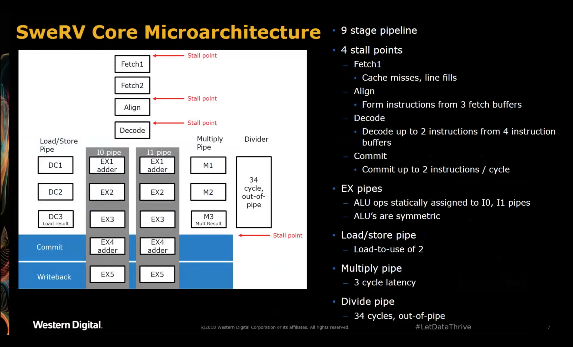
SweRV Core Microarchitecture
-
Superscalar Design
The SweRV was designed to replace existing CPU cores in Western Digital SOCs. For their uses cases, single threaded performance is critical. That’s why they chose a 2-way superscalar pipeline, even if 2 separate CPUs with a traditional 5 stage RISC pipeline would require less resources, less power, and higher aggregate performance.
They also have a lot of code where some of the code is Western Digital proprietary while others is written by customers, with no easy way to separate things into concurrent threads.
The superscalar architecture provides a purely theoretical performance increase of 100%, but real world workloads show a boost between 25% and 30%.
-
Second set of ALUs
When both operands are already available, ALU operations are executed during the
EX1stage. However, if this ALU instruction is dependent on a register load instruction before, the ALU operation is not executed duringEX1but passed along toEX4where it has a second chance to be executed.Western Digital uses pipelined RAMs with a 2-cycle access latency. When the core issues a register read in the
DC1stage of the load/store pipeline, the result will arrive 2 cycles later, just in time to be used by the ALU in theEX4stage.The net result is that the core was able execute an dependent instruction without the need to insert a bubble.
According to the presenter, this second set of ALUs increases the performance of the core by a whopping 50%. I think this number is stunning. So much so that I still can’t quite believe it to be true. It’d be very interesting to put this claim to the test and modify the RTL to disable this retry-ALU.
-
Load/Store Unit
There’s only one LSU. Two LSUs were considered, but the additional complexity, resources and power where not an appealing trade-off for an embedded core.
-
Minor Out-of-Order Capability
The slide show at the May 2018 workshop mentions “mostly in-order core”. The reason for this is that loads do not block the core until the point where the register value is needed in the pipeline. This can give a nice additional boost but support from the C compiler is necessary to really exploit the potential.
-
Multiplier
As can be seen: spread over 3 cycles in a parallel pipeline.
-
Divider
An iterative out-of-pipeline divider that has a worst-case performance of 34 clock cycles. In practice, due to various optimizations and depending on the operands, the average division takes around 15 to 17 cycles.
-
No Support for Instruction Fusion or Macro-Op Fusion
In his presentation at the July 2016 RISC-V workshop, David Patterson made the case of macro-op fusion as a way to avoid ISA bloat. Macro-op fusion is a feature of the micro- architecture of a CPU where multiple standard ISA instruction are merged by the decoder into one single instruction.
For example,
CMP, BNEis merged into a single instruction.Macro-op fusion is implemented in some of the Berkeley RISC-V cores (such a BOOM), but not implemented in the SweRV “because it doesn’t fit the SweRV ideology.”
SweRV Pipeline Diagram
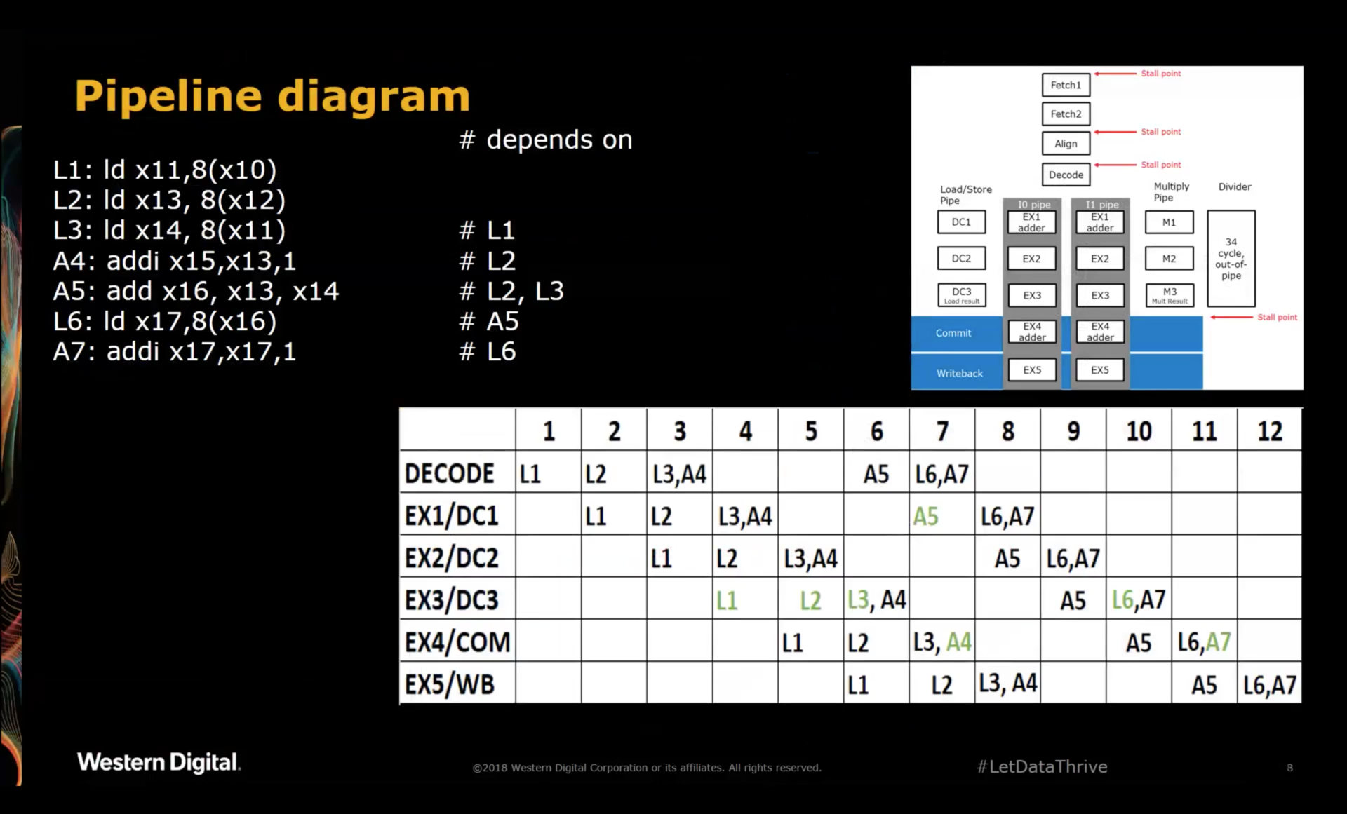
The presentation had an example with a traditional pipeline diagram to clarify how certain instruction combinations are issued and stalled in the pipeline.
In the diagram above, green indicates a successful execution of an instruction.
To get a better idea about what’s going on per instruction, I have edited the pipeline diagram with some additional annotations.
Let’s first look at instruction A4:
A4 is dependent on x13, the result of load L2. At cycle 4, the first chance for A4 to execute in stage
EX1, L2 is still 2 cycles away from having the contents of x13 available.
Instead of stalling the pipeline, A4 travels further down the pipeline until it reaches stage EX4 where it
gets its second chance at executing. At that point, the result of L2 is present in stage EX5, ready to be
written to the register file.
If the pipeline diagram correctly reflects that architecture of the SweRV core, there’s a forwarding path
from EX5 to EX4, which allows A4 to use the result of the L2 instruction.
We can see in the diagram that no bubbles were inserted between L2 and A4, something that would have been
impossible without the EX4 retry stage: a hypothethical SweRV core without retry ALU units would have
required a bubble of 1 clock cycle: sufficient to line up L2 at the EX1 stage on cycle 5, when the result
of L2 is first available.
The situation for A5 is easier:
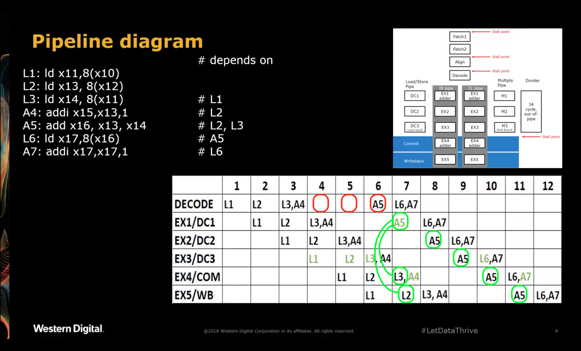
A5 depends on the results of L2 and L3. According to the diagram, the CPU stalls A5 until the results of
L2 and L3 are available in EX4 and EX5 respectively. Thanks to forwarding paths from EX4 and EX5
to EX1, the CPU can execute A5 during cycle 7.
After that, A5 execution is complete and it can sail through the remainder of the pipeline until the
result gets written into the register file one cycle 11.
Note that with a forwarding path from DC3 to EX1, A5 could have launched into the pipe one cycle earlier,
thus reducing the number of bubbles from 2 to 1 cycle. Based on this diagram, such a forwarding path does
not exist. The delay from clock to output of RAMs can be notoriously bad, and it’s often in the critical path
of a design. However, that should have been mitigated by having a 2 cycle latency for a RAM access. The
decision to forgo this forwarding path was probably another trade-off between logic, power and performance.
Finally, A7 presents another case where the ALU of EX4 saves the day:
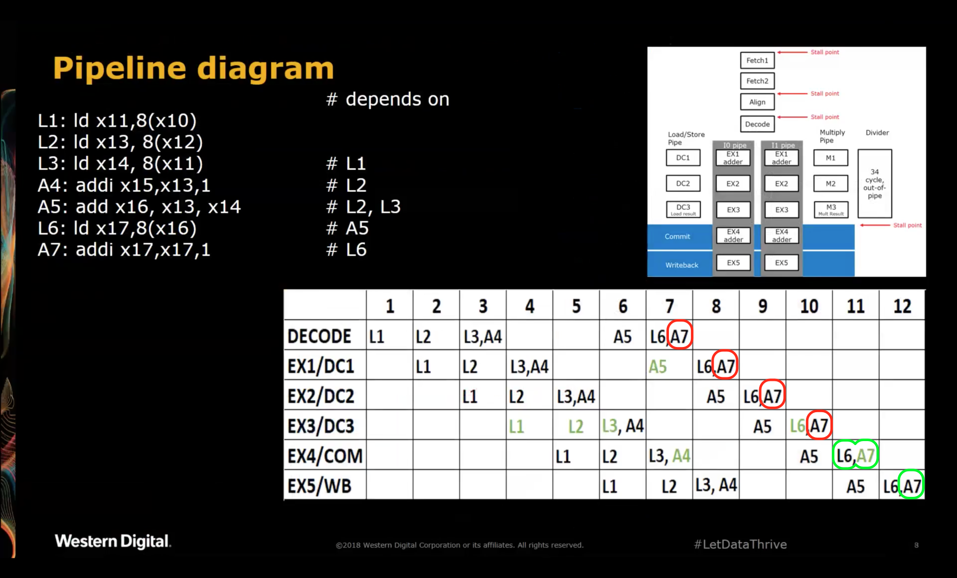
Contrary to A5, A7 depends on the result of the load instruction that comes right before it. As a result,
A7 reaches EX4 right at the same time as the result of L6. There is no forwarding path necessary: A7
can simply grab the result of L6 as operand from the same pipeline stage and execute.
SweRV Core Branch Prediction and Handling
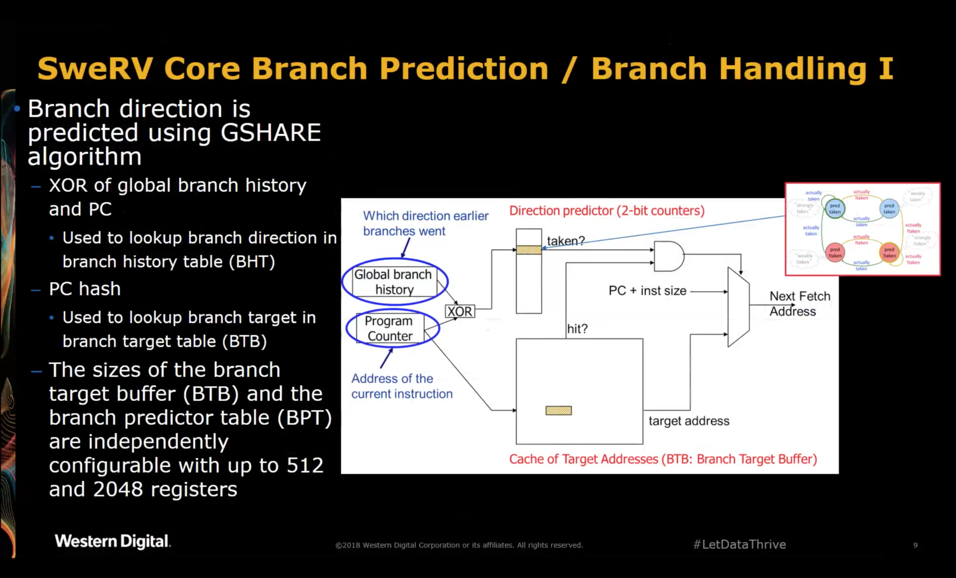
The SweRV uses the GSHARE branch prediction algorithm. According to the presenter, the architects didn’t have a lot of choices: the majority of open source cores such as those from Berkeley and ETH Zurich, as well as commerical cores all use GSHARE. Doing anything less complicated would cripple the performance compared to those cores, and more complicated algorithms are unreasonably expensive to implement.
A Google search for the GSHARE algorithm gives tons of links with information.
As is the case for many other SweRV parameters, the number of entries in the branch prediction table can be sized based on performance needs.
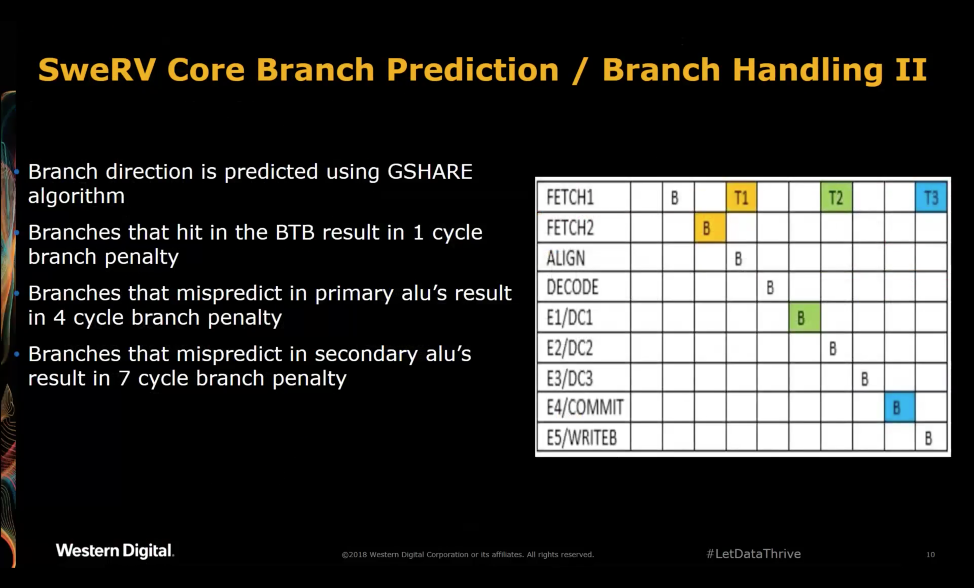
The biggest negative consequence of the retry ALU is the fact that mispredictions that are only apparent after EX4 result
in a 7 cycle branch penalty!
SweRV Instruction Set Simulator
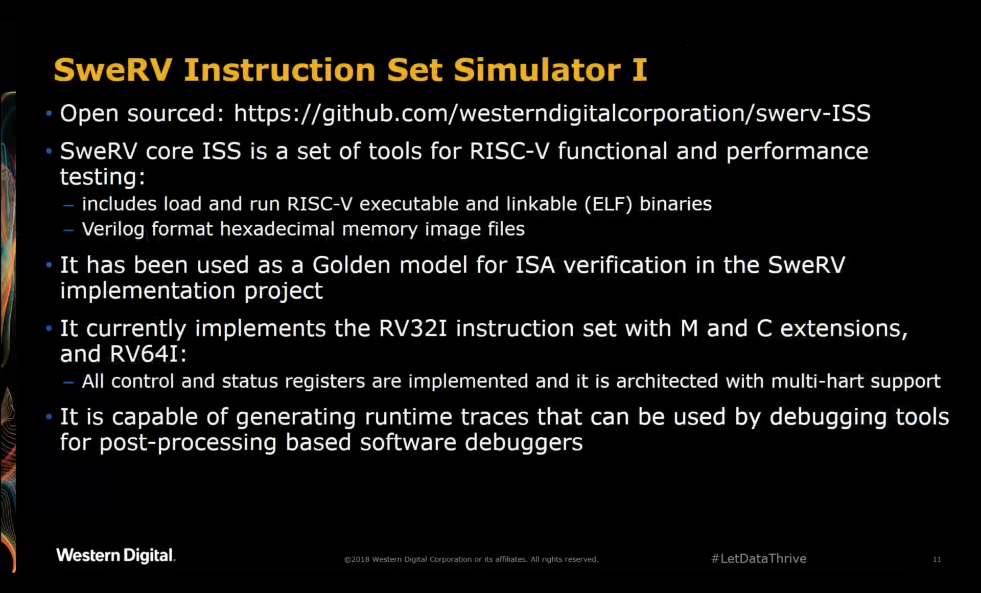
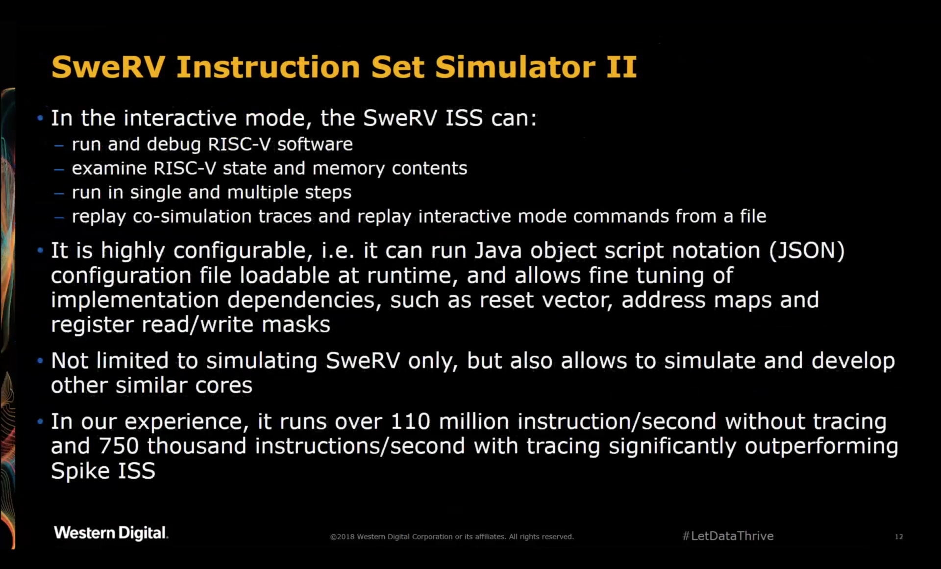
In addition to the SweRV RTL, Western Digital also open sourced their instruction set simulator. Not too much additional detail was given than what was on the slides.
They decided to write their own ISS instead of using Spike because Spike didn’t exactly fit their needs. They have many man-years of experience doing ISS. Getting this one up and running only took about a week.
The ISS can easily be modified for different cores.
The source code is here.
Since the ISS is used to generate traces that are used to verify the RTL, I was wondering if the ISS also has all the microarchitectural details (the superscalar nature etc.) So far, I’ve not been able to identify where this is specified.
SweRV Physical Design
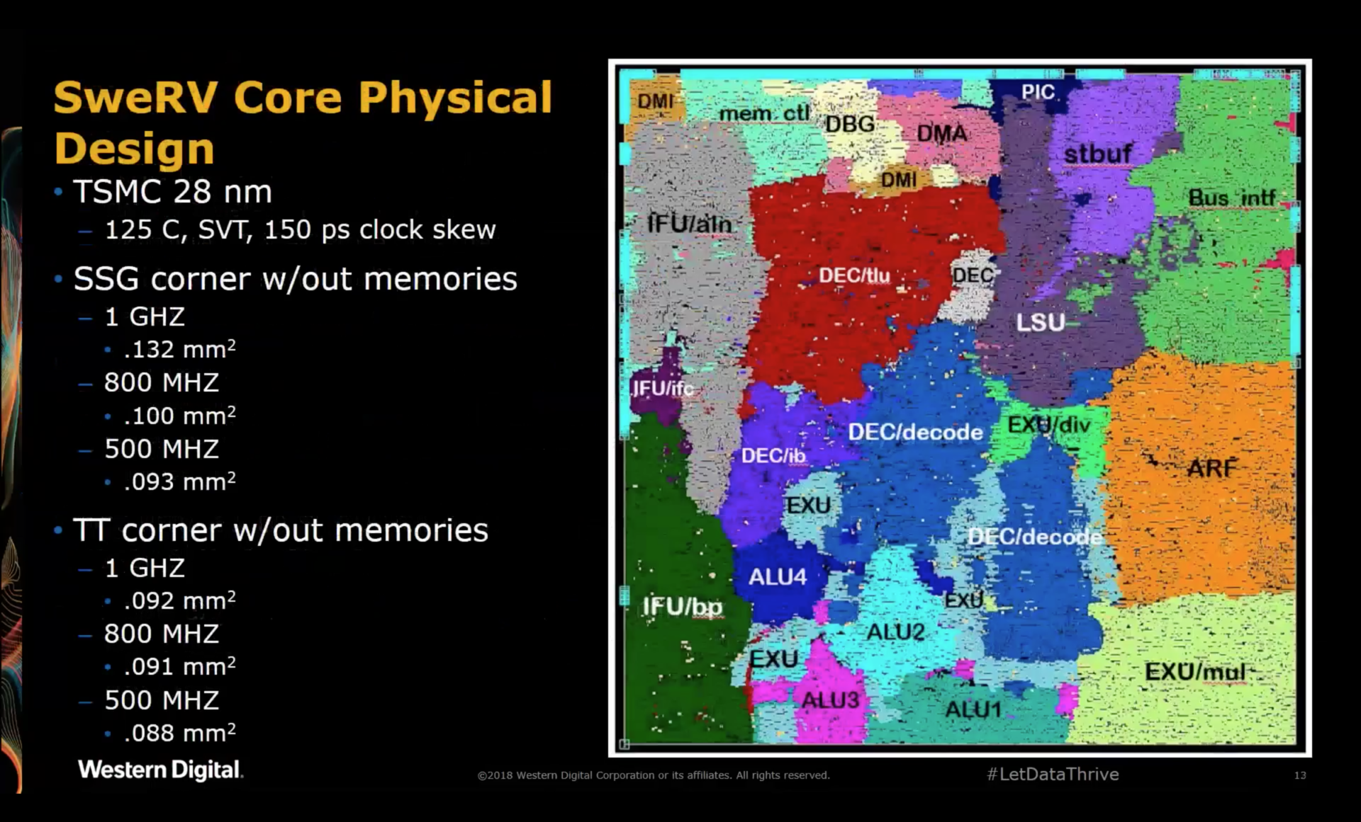
According to the presenter, legal told him to remove the labels on the individual regions, but the same slide was presented, with labels, at the RISC-V workshop, so I think it’s all good. :-)
The initial budget was 0.180 mm2 for the core (without RAMs). The final result is well below that.
SweRV Core Performance
A CoreMark score of 4.9 CM/MHz is excellent, but already stale: with additional optimizations, their number now stands at 5.0.
Going higher than that would require a significant investment in terms of logic and branch prediction.
As mentioned earlier, the SiFive E76 core claims a score of 4.9 CM/MHz as well with an 2-way superscalar 8-deep pipeline. The Core Complex Manuals of various SiFive cores can be found here.
Like the SweRV, the E76 also gives arithmetic instructions a retry opportunity, since they can be executed either
in the AG stage or the M2 stage.
Correctly predicted branches and direct jumps result in no penalty, provided the target is 8 byte aligned, while the SweRv has a 1 cycle penalty for correctly predicted jumps.
All in all, the E76 and the SweRV are very similar, with very similar performance as a result.
RISC-V Code Density and Optimization
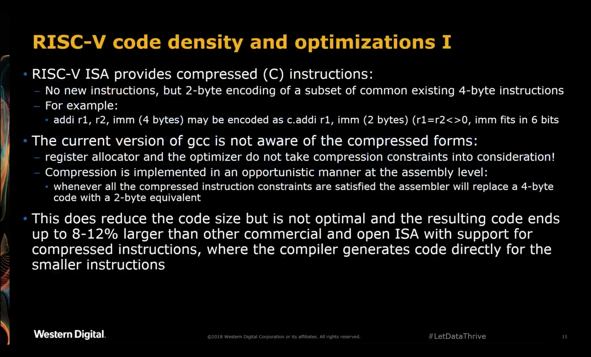
Because of the inefficient way in which GCC currently generates compressed instructions, code density isn’t as good as it should be, with binaries that are between 8 and 12% larger than their previous CPUs.
They are working with the RISC-V consortium to improve GCC’s compressed instruction generation. Code will be upstreamed, of course.
Meanwhile, they are using compiler flags to reduce code size:
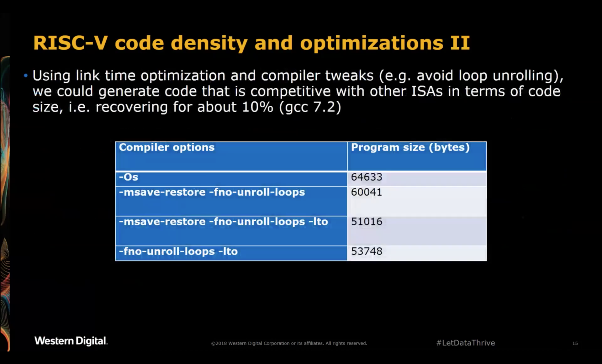
In the numbers above, the original RISC-V code size is 64KB, compared to 51KB for their older chips with commercial CPU. (They don’t use GCC for that CPU.)
With additional compiler options, they can recoup most of the code size:
-
-msave-restoreThis options replaces the entry and exit code of a function where registers are saved and restored by a function call. My personal experience is that compared to ARM, which has LDM and STM load/store multiple operations, RISC-V wastes a lot of code space on this.
-
-fno-unroll-loopsSelf-explanatory…
-
-ltoLink Time Optimization takes in a higher level view of the code as opposed to assembler instruction when linking. This allows it to make some additional optimizations that would otherwise not be possible.
According to the presenter, a negative of LTO is that there were issues getting the debugger to deal with it correctly.
Various
They saw a lot of interest after the public release. One question is how to deal with pull request and how to integrate that with their internal design flow.

SweRV for Hobby Use?
I’m still in the early stages of going through the SweRV RTL and ISS, but it’s clear that SweRV is not a good fit to stick in an FPGA for hobby projects:
- The register file has 4 read ports and 2 write ports. This makes it necessary to use FFs instead of RAMs, and it’s very wasteful on an FPGA.
- During their demo of the SweRV on an Artix 7 FPGA, they were able to reach a clock speed of around 40MHz, with the critical path being in the decoder. This is not really a surpise: FPGAs are not very good a large blobs of combinatorial gates, and superscalar architectures add additional complexity. A VexRiscV, which was designed for FPGA, would run circles around a SweRV in terms of clock speed, probably enough to outweigh the better IPC fo the SweRV.
- The RTL is written in SystemVerilog, using some constructs like port assignment wildcards that are not (yet) supported by Yosys. This eliminates open source flows as a potential candidate.
- Finally, the SweRV core is big: it’d probably fill up 50% of a relatively large Artix 7 FPGA, though that needs to be tested in practice.
Formal Verification
After the presentation, I asked about formal verification of the core. Zvonimir confirmed that they used formal
methods at a later stage and that “they found some nasty bugs”. The code that was released on GitHub has no signs
of Clifford Wolf’s RVFI interface that is defined in the riscv-formal
project, so it’s not clear what kind of test suite was used to verify the correctness.
Parting Thought about Performance
When you have a look at the SweRV architecture and implementation, it is not incredibly complex, especially compared to, an out-of-order triple-issue A-15 core. And yet it achieves similar or higher CoreMark/MHz scores. Is this because of the memory system, where most CoreMark measurements are done with a DRAM system instead of fixed latency on-chip SRAM? But even if we stay within the RISC-V family and compare against the Boom v2, with the similar scores, but also a much more complex OOO architecture (requiring, for example, a 9 read port/3 write port register file), the score is remarkable.
I’d love to learn more about that!
I would like to thank the Bay Area RISC-V Group for organizing this deep dive, and Western Digital for hosting the meeting, providing the content, and releasing the source code on GitHub!