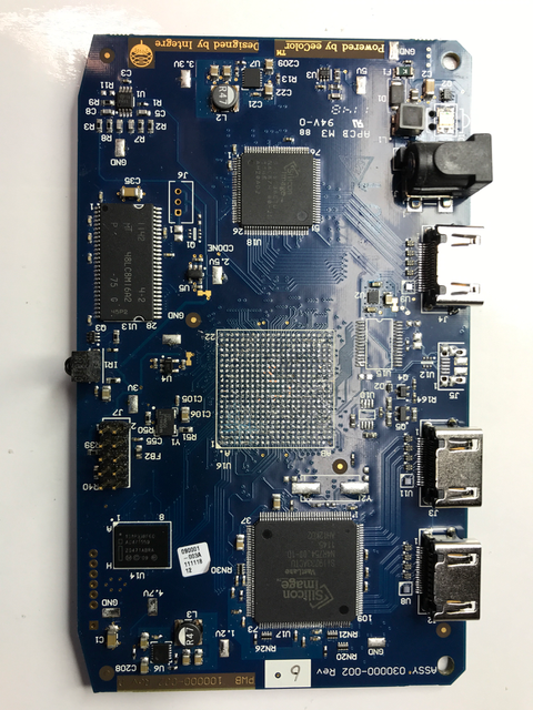
eeColor Color3: SiI9136 and SiI9233 Connections to FPGA
Most of the connections that matter were already mapped by others, except for the SiI9136 and SiI9233 connections. Those are really interesting chips if they can be made to work, so that’s what I’ve been doing the past few days.
I used the technique that I described earlier: using a super wide input signal that’s connected to a signal tap with an OR-trigger, and then tapping a grounded resistor to the input pins.
That works very well for pins that are supposed to be driven by the FPGA. In other words: it works great for the signals of the SiI9136, since that’s an HDMI TX chip that receives data from the FPGA.
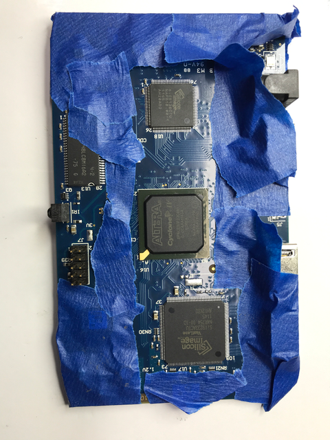
Until… it doesn’t work anymore. While I was mapping the signals, Quartus suddenly lost connection with the board and it never recovered. I vaguely remember making an uncontrolled move shortly before that, during which I may have touched the power regulator with my probe (a resistor).
Long story short: I blew up the board.
Luckily, I had already ordered another one on eBay a few days earlier because somehow I knew that I would screw things up one way or the other! (Meanwhile I’ve ordered yet another one, just in case.)
With virtually all connections on the FPGA hidden under a BGA package, I would have been stuck, were it not for the fact that, a month or two ago, I had ordered a hot air desoldering+soldering station. (A full featured desoldering station from a cheap brand was cheaper than a soldering-only station from an expensive brand.)
Since I now had a dead board anyway, this was an excellent opportunity to use the station for the first time!
It worked great. After a few minutes, I had the following result:
With the FPGA gone and the TQFP pins of the SiI chips, I could now just Ohm out the connections.
On the still working color3 board, I’m now taking the right precautions when experimenting:
I can now clumsily handle my probes with almost no risk of accidentally touching Things That Should Not Be Touched.
There are still one or 2 pin assignments that don’t quite make sense, but the pin mapping process is essentially complete and checked in as a .qsf file on GitHub.
Next step: create a small design with a Nios2, an I2C master to control the SiI chips, and a video test image generator. If all goes well, I should have a HDMI image on my monitor in a few days.
How hard could it be?
References
All posts in this series: