Getting Started with ECP5 FPGAs on the Colorlight i5 FPGA Development Board
- Introduction
- The Colorlight i5 Module
- Features of the Muse Lab Development Board
- First Impressions
- Design Documentation
- From Unboxing to Blinky
- Programming a Bitstream into SPI flash
- Other Demo Bitstreams
- From Verilog to Bitstream
- Using the Board for Your Own Projects
- Conclusion
- References
Introduction
There are hundreds of FPGA development boards out there, and I don’t dare to count but I must own a considerable fraction of them. Most of these are designed deliberately for development purposes, but a few are not, and yet they can sometimes be a good match.
One board that falls in this category is the Colorlight i5.
Like other members of the Colorlight family (the Colorlight 5A-75B comes to mind), the i5 is ‘real’ product that is designed for one specific purpose: it is a controller for large LED video panels. And that’s a huge plus, because in FPGA land, high volume means low cost, usually much lower than buying individual components on Digikey or Mouser.
The Colorlight i5 is especially attractive because it’s a plug-in card, with a reappropriated DDR SODIMM connector. Even better is that nothing about this module seems to be tailored specifically for LED panels. Unlike the 5A-75B, there are no unidirectional 3V3 to 5V level shifters: FPGA GPIO pins are routed straight to the SODIMM connector and can be used any way you want: input or output, LVCMOS or LVDS or any configuration that’s supported by the FPGA.
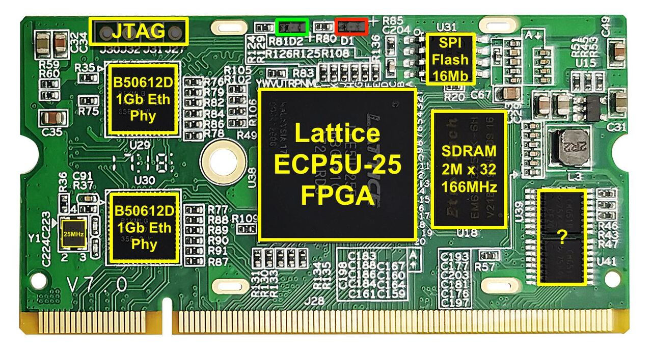
The Colorlight i5 uses a Lattice ECP5U-25, an FPGA that’s supported by the Yosys/NextPNR open source tool flow, an extra bonus. The board is also supported by recent versions of Icestudio.
That said, there’s still a hurdle to using this board as development platform: you need a way to power it, there are no easy usable GPIO connectors (such as PMOD connectors), and while are easily accessible test JTAG points to program the FPGA, you still need an external JTAG programmer and solder a bunch of wires to make things work.
Or…
you could go to the AliExpress webstore of Muse Lab and buy their Colorlight i5 development board.
Muse Lab also sells a number of other interesting hobby FPGA boards, such as the ICE40 UP5K based iCESugar, but the ECP5 FPGA on Colorlight i5 has a much larger capacity, so I bought their module + development board combo for $50 and gave it a try.
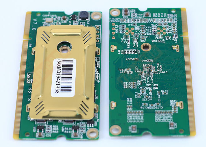
The Colorlight i5 Module
Skip to From Unboxing to Blinky if you want to get your hands dirty ASAP.
Let’s first go over characterstics of the module itself:
-
Low Cost: $30 and up
I’ve seen these modules for $18.50, but with a $25 shipping fee, which makes it only attractive if you’re buying at least 3. For $35, you can get them with free shipping on AliExpress. That’s still a fantastic deal for what you get.
-
Lattice ECP5 LFE5U-25F FPGA
Specifications:
- 24K LUTs
- 56x sysMEM block RAMs (of 18Kb each), good for up to 126KByte of on-chip RAM
- 194Kb of distributed RAM
- 28x DSPs with 18x18 multiplier and 36-bit accumulator
- 2 PLLs, 2 DLLs
- 0 SERDES
- 381 caBGA package
The -25 version is one of the smaller versions in the ECP5 family, but it’s still enough for many applications. You can comfortably fit a VexRiscv-based Linux SOC in there.
-
EtronTech EM638325-6H 2M x 32bit SDRAM, 166MHz
Single data rate SDRAM is ancient and slow now, but sufficient for most hobby projects. It’s also easier to use because there’s usually no trickery required with complex PLL/DLL configurations.
-
2x Broadcom B50612D 1Gb Ethernet Transceivers
That’s right, not one but two. You could make your own firewall with this thing.
The PHYs are using an RGMII MAC interface.
The module only contains the transceivers, not the Ethernet transformers or RJ45 connectors. The 2x 4 differentials pairs are routed to the SODIMM pins.
Check out this Ethernet expansion board by Kazumoto Kojima:
-
GD25B16C 16Mbit Quad SPI Serial Flash
According to the Lattice ECP5 sysCONFIG Usage Guide, the FPGA has a maximum uncompressed bitstream size of 5.42Mb. That leaves more than 11Mb or ~1.4MByte for user applications.
-
25MHz Oscillator
The Ethernet transceivers require a 25MHz oscillator. It also goes to the FPGA as its only external clock input.
-
2 LEDs
A red LED seems to be connected to power and is always on, but the green LED is controlled by the FPGA: a strict requirement to get that blinky going!
-
JTAG Interface
4 JTAG test points are not marked as such but they are easy to solder and accessible.
-
3x Mystery CD4051B 8 Channel Analog Multiplexer/Demultiplexer
These are only present on V7.0 of the board, not on V6.0. Its functionality hasn’t been reverse engineered yet, but some of the demultiplexed ports are going to the SODIMM pins.
-
DDR-SODIMM Connector
-
3V3 to 6V power rail
There are voltage regulators on the module, but there are no pins back to the connector with regulated voltage.
- 2x 4 differential Ethernet pairs
- 106x general purpose GPIO pins
-
2 mystery
RCV_BK1/RCV_BK2pinsThese have something to do with receiver backup power. Unknown how they are connected on the module.
-
21 mystery pins
Related to the 8 channel analog multiplexers.
-
-
A heat sink
Not exactly a heavy duty one, but a piece of metal that squeezes against the FPGA and the two Ethernet transceivers. Much better than nothing!
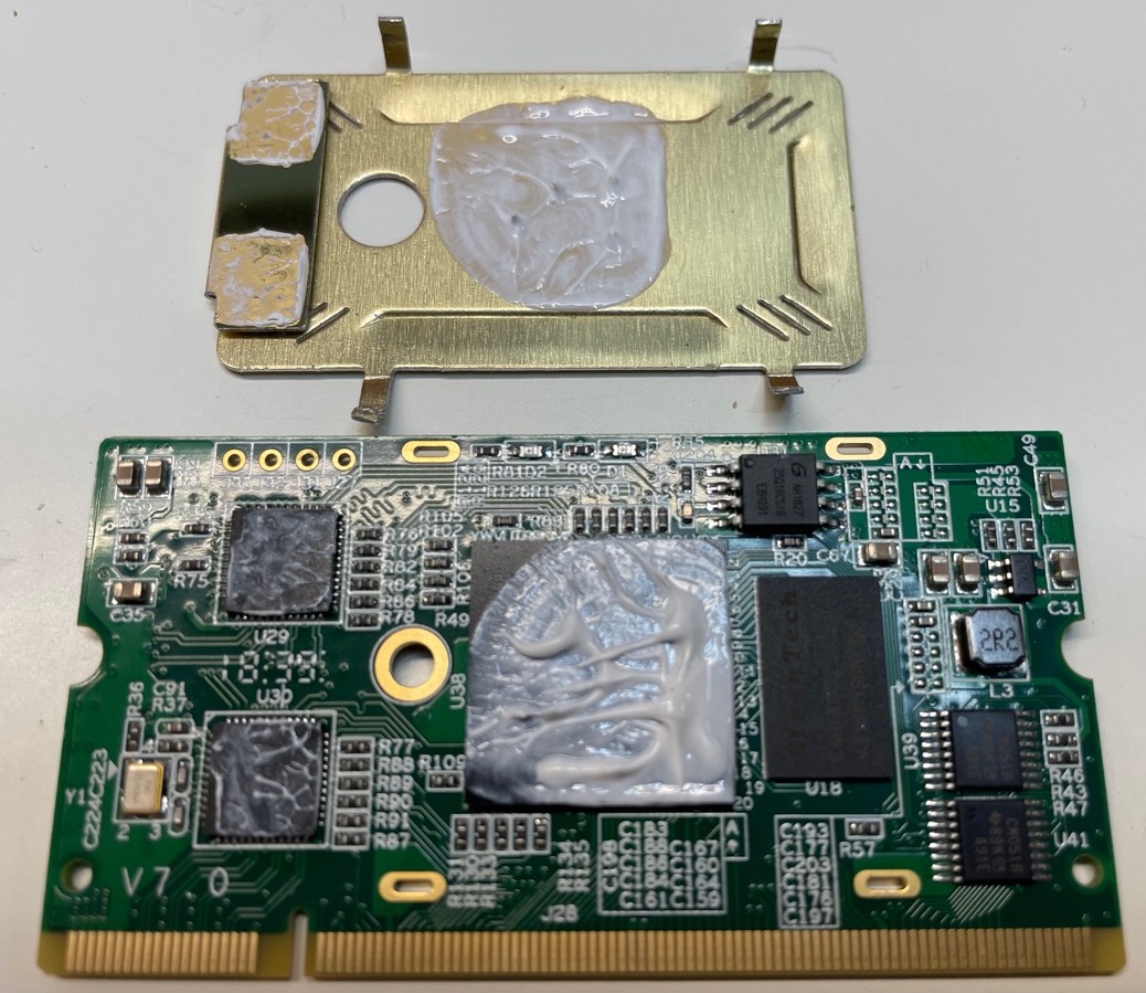
The heat sink is pretty easy to remove without damaging the board.
There’s a lot to work with here. What’s even better is the potential for future upgrades: Colorlight has i6, i9, and i9+ modules with the same SODIMM pinout as the i5, but with larger FPGAs: the i9 board has a Lattice ECP5-45. The i9+ a Xilinx Artix A50T.
For the i5 board, V6.0 and V7.0 are pinout compatible too, with the exception of the mystery pins.
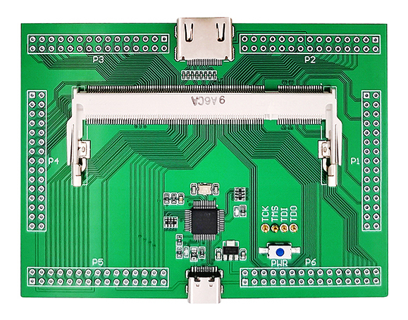
Features of the Muse Lab Development Board
As I wrote earlier, the development board can be bought on AliExpress, but only as a package deal: $50 for the development board and the i5 module, with free shipping.
It has the following features:
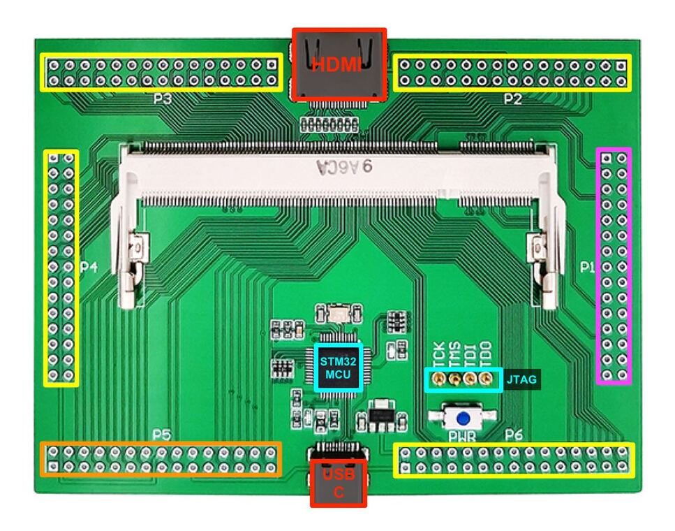
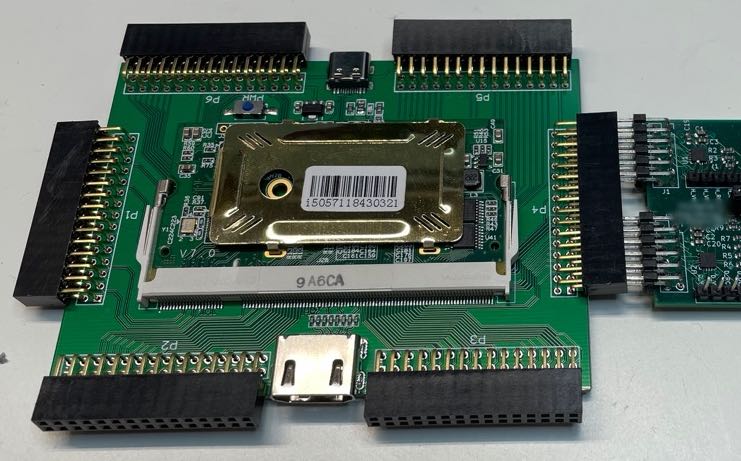
- DDR-SODIMM socket for the i5 module
-
1x 30-pin connector for Ethernet (purple)
This connector has the 2x 4 differential Ethernet pairs.
-
4x 30-pin connectors for generic GPIOs (yellow)
Each connector has 20 GPIOs, ground, 3V3, and 5V pins. The pins are smartly organized so that the connector is also compatible with 2 side-by-side PMOD connectors.
In this case, the center pins can’t be used and the number of usable GPIOs per 30-pin connector drops to 16, 8 for each PMOD.
-
1x 30-pin mixed-use connector for generic GPIOs + special functions (orange)
Just like the 4 earlier connectors, there are 20 GPIOs on this connector, in the same configuration, but 6 of the GPIOs have been assigned a special meaning: UART and SPI.
The UART and SPI pins are also routed to the microcontroller to be used as a potential FPGA debug console, and, presumably to progam the SPI flash on the board.
As I write this, the MCU doesn’t use the SPI pins, so it’s something that could be used, in theory, for data transfers between the FPGA and MCU ( and then the host PC) at higher rates than the UART. But this would obviously require custom STM32 firmware.
-
HDMI connector - video out only
This one is a surprise, since the FPGA on the module does not support high speed SERDES IOs. Instead, the pins are connected to generic IOs that can be configured as differential pairs inside the FPGA.
I doubt that these IOs meet the strict electrical requirements that are set by the HDMI standard specification, but meeting these requirements is not necessary to drive an image that can be decoded by most monitors.
Unfortunately, the I2C, HOTPLUG and CEC pins of the HDMI connector are not connected. The lack of HOTPLUG makes it impossible to use the HDMI connector for video input.
-
USB C Port
A USB C port is used to power the board, to program the FPGA, and to send FPGA UART console traffic from and to a host PC.
-
STM32F103C8T6 microcontroller (MCU)
This STM32 MCU is identical to the one used on the dirt cheap and popular Blue Pill development boards.
The MCU on this development board is used as programming and debug interface only. On one side, it has a USB 1.1 interface to connect to a host PC. On the other, it controls JTAG, UART, and SPI pins to the Colorlight module. It also controls 2 LEDs.
The user is not supposed to reflash the MCU with custom firmware, but if you’re so inclined, the SWD pins to do so are located underneath the USB connector (on the other side of the PCB.) You’d need one of those STLink programming dongles that I wrote about a couple of years ago. If you even need to reflash the STM32 firmware to it original stage, you can find the binary image here.
-
USB 5V -> 3.3V voltage regulator
An AMS1117-3.3V that’s used to convert the USB 5V to 3V3 to power the MCU and the 3v3 pins of the PMOD ports, but NOT the Colorlight module (which is powered by USB 5V rail and has its own voltage regulators.)
-
2 LEDs
Not to be confused with the 2 bright LEDs on the module itself, two tiny and faint LEDs are controlled by the MCU. The red LED flickers when there’s USB traffic. A blue LED seems to be always on and is hidden entirely underneath the module.
-
Power Button
When pressed, this button interrupts power to Colorlight module, but not to the MCU. If you want to power off the MCU, you must unplug the USB cable.
-
JTAG Pogo Pins
While the i5 module has easy accessible JTAG test points, they are not connected to the SODIMM connector. The development board makes the connection with the test points with 4 pogo pins. It’s an elegant solution that removes the need for any soldering.
First Impressions
The package arrived with the i5 module (V7.0), the development board, a USB C cable, and 6 30-pin connectors that you need to solder yourself.
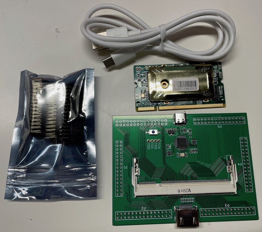
I’m not well qualified to judge the quality of the PCB, but it looks well made to me.
After inserting the 30-pin connectors into the PCB (it’s a bit of a hassle that requires wiggling slightly bent pins in the right hole), I noticed a minor issue: my HDMI cable doesn’t fit between the 2 30-pin connectors that surround the HDMI connector. As a result, the cable can’t be plugged in completely:
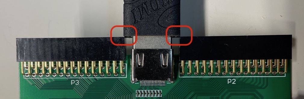
You need a HDMI cable with a narrow connector to make things work, or don’t solder connectors P2 and P3, which is what I did.
The box doesn’t contain any documentation, not even a leaflet with a URL. You have to make do with Google or a link on the AliExpress product page to a GitHub repo.
Without further instructions, I plugged the USB cable into the board and my PC, some LEDs came up and I heard a little sound: my PC told me that it had seen a new “DAPLINK” USB drive. So far so good!
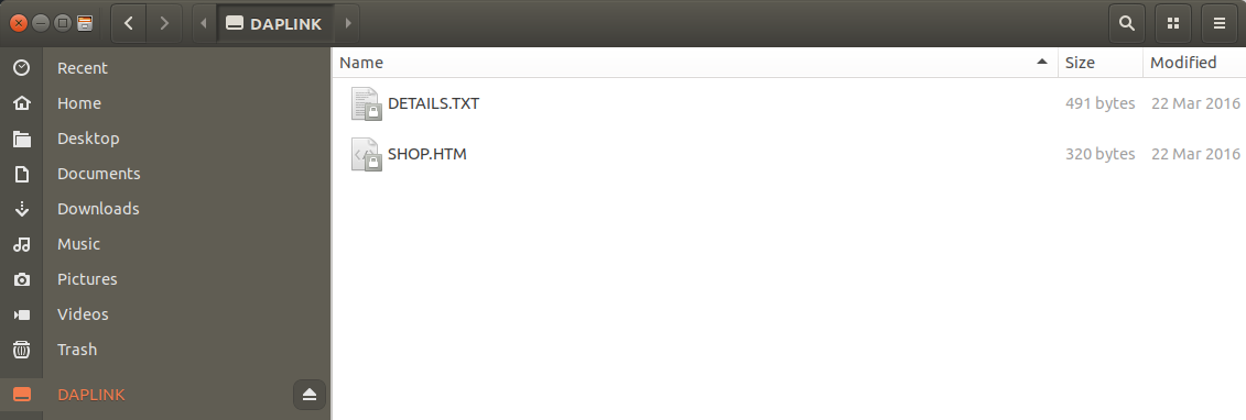
I didn’t find any use of this USB drive. It’s supposed to enable flashing a binary through simple drag-and-drop, but that functionality doesn’t work for this board.
Design Documentation
As I write this, there are 2 main sources of information about the development board:
-
A GitHub repository that’s maintained by the creator of the board. Let’s call this the official board documentation.
The repo covers the following topics:
- a Getting Started document
- pin assignment of FPGA IOs
- schematic of the development board
- datasheets of the module components and more
- source code of demo designs and their precompiled bitstreams
- tools to program and flash the FPGA
The demo designs borrow heavily from Radiona’s ULX3S FPGA development board. In many cases, source code is a straight copy with just FPGA pin assignment changed.
The same is true for the
toolsdirectory (for example, it containsujprogwhich stands for “ULX3S JTAG programmer”). I won’t be using any of these tools, however, because I found a better option usingecpdap. See below. -
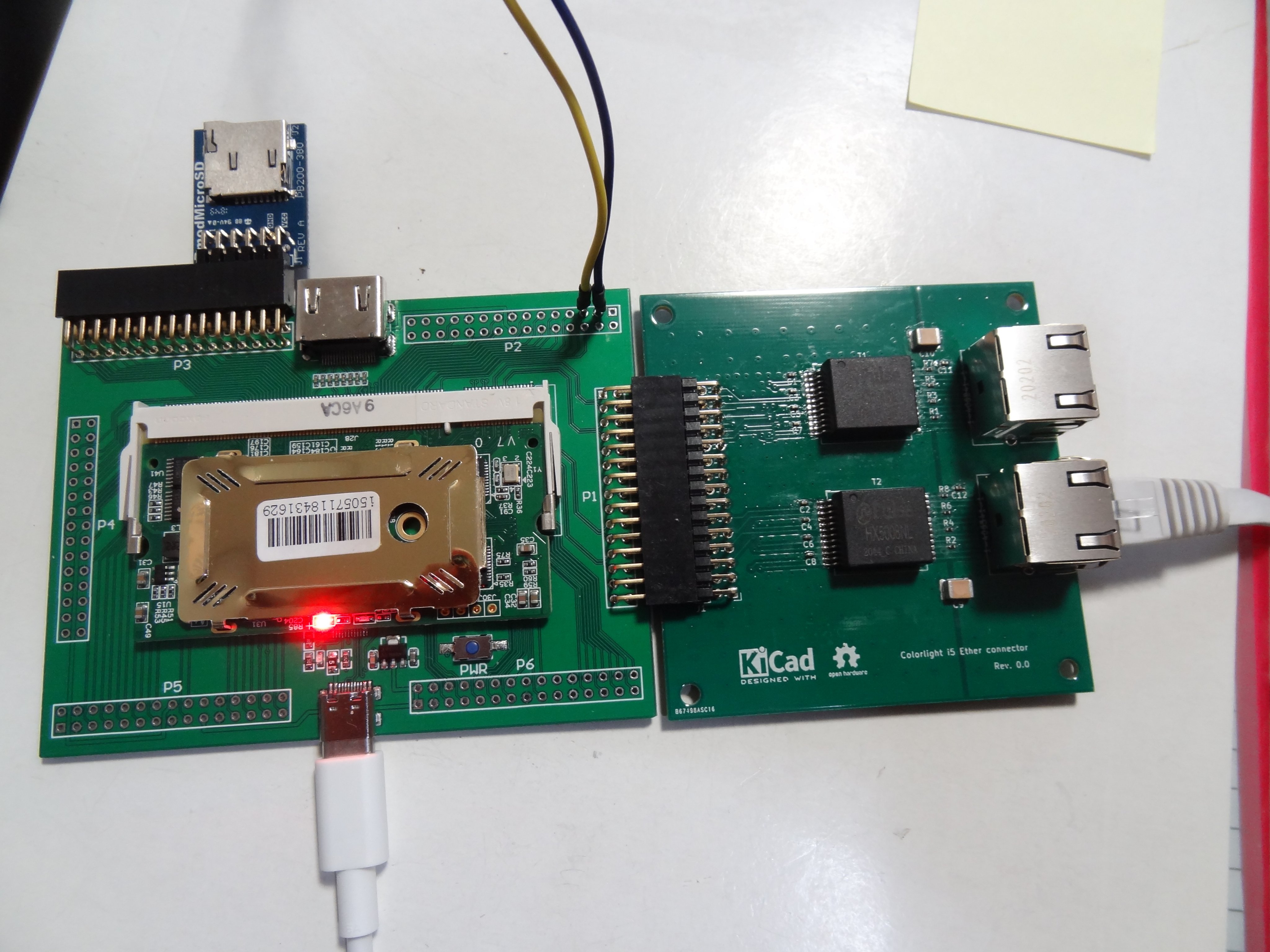
A non-official repo that covers a variety of topics. From instruction on how to unlock the SPI flash (I’ll cover that part later), to adding an Ethernet expansion board, to running Linux on a VexRiscv based soft core CPU on the FPGA.
I’ve reverse engineered and brought up a number of FPGA boards that didn’t have any documentation at all, so getting a Colorlight i5 to work with at least some documentation wasn’t an issue, but it’d be a challenge for a beginner or somebody less experienced.
What follows are my notes on getting from unboxing to running an LED blinky, with all steps explained along the way.
From Unboxing to Blinky
The normal sequence of things is to go from Verilog to synthesis to place-and-route to loading a bitstream.
However, since the official GitHub repo already contains demos with prebaked bitstreams, I will start with loading one of those first.
I’m assuming you’re using a Linux system. I’m running Ubuntu 18.04.
The official GitHub repo suggests using OpenOCD and their own tool dapprog to load bitstreams and program the
SPI flash. I’m using Adam Greig’s ecpdap instead:
it has more features, it’s easier to use, and it’s faster.
Step 1: Clone the GitHub repo
git clone https://github.com/wuxx/Colorlight-FPGA-Projects.git
Step 2: Download ecpdap
ecpdap is a tool that makes your PC talk to the STM32 controller on the development board. It uses
the CMSIS-DAP protocol to download bitstreams, erase the i5 SPI flash,
program the flash etc.
The ecpdap repo is here. You can compile it from source (it’s written in Rust), or you can download a binary release, which is what I did. Make sure you use release v0.1.5 or later. Earlier versions didn’t play well with the Colorlight development board.
Move the ecpdap to some location in your $PATH of your choice, such as /usr/local/bin.
Step 3: Get everything ready for use
- Plug in the Colorlight i5 module into the development board
- Connect the development board to the PC with the USB cable
-
Check that the board is connected correctly
The most comprehensive way is to do this is to check the kernel messages with dmesg after plugging in the board:
> dmesg -w
[3188607.164686] usb 1-11.2: new full-speed USB device number 57 using xhci_hcd
[3188607.279905] usb 1-11.2: New USB device found, idVendor=0d28, idProduct=0204, bcdDevice= 1.00
[3188607.279908] usb 1-11.2: New USB device strings: Mfr=1, Product=2, SerialNumber=3
[3188607.279910] usb 1-11.2: Product: DAPLink CMSIS-DAP
[3188607.279911] usb 1-11.2: Manufacturer: ARM
[3188607.279913] usb 1-11.2: SerialNumber: 070000010670ff495356675287180632a5a5a5a597969908
[3188607.300937] usb-storage 1-11.2:1.0: USB Mass Storage device detected
[3188607.301467] scsi host6: usb-storage 1-11.2:1.0
[3188607.302123] cdc_acm 1-11.2:1.1: ttyACM0: USB ACM device
[3188607.304590] hid-generic 0003:0D28:0204.0039: hiddev0,hidraw4: USB HID v1.00 Device [ARM DAPLink CMSIS-DAP] on usb-0000:00:14.0-11.2/input3
[3188608.329624] scsi 6:0:0:0: Direct-Access     MBED     VFS              0.1  PQ: 0 ANSI: 2
[3188608.329962] sd 6:0:0:0: Attached scsi generic sg1 type 0
[3188608.330509] sd 6:0:0:0: [sdb] 131200 512-byte logical blocks: (67.2 MB/64.1 MiB)
[3188608.330780] sd 6:0:0:0: [sdb] Write Protect is off
[3188608.330782] sd 6:0:0:0: [sdb] Mode Sense: 03 00 00 00
[3188608.330973] sd 6:0:0:0: [sdb] No Caching mode page found
[3188608.330976] sd 6:0:0:0: [sdb] Assuming drive cache: write through
[3188608.354134]  sdb:
[3188608.355706] sd 6:0:0:0: [sdb] Attached SCSI removable disk
There’s a lot going on here. The USB port presents multiple USB interfaces.
-
usb-storage 1-11.2:1.0: USB Mass Storage device detectedThe board acts like a USB drive. (See above. We will not be using this.)
-
cdc_acm 1-11.2:1.1: ttyACM0: USB ACM deviceThere’s a serial port that will be used to bridge a UART on the FPGA (when there is one) to the PC.
-
hid-generic 0003:0D28:0204.0039: hiddev0,hidraw4: USB HID v1.00 Device [ARM DAPLink CMSIS-DAP] on usb-0000:00:14.0-11.2/input3CMSIS-DAP is the protocol that’s used to send JTAG, SWD, and other debug protocols from the PC to the MCU.
-
Step 4: Verify that ecpdap can talk to the board
Check that ecpdap finds the STM32 MCU:
$ ecpdap probes
Found 1 CMSIS-DAP probe:
  0d28:0204:070000010670ff495356675287180632a5a5a5a597969908 DAPLink CMSIS-DAP
Check that ecpdap can find the ECP5 FPGA:
$ ecpdap scan
Detected JTAG chain, closest to TDO first:
 - 0: 0x41111043 ECP5 LFE5U-25 [IR length: 8]
That was easy!
Step 5: Load a blink bitstream to the FPGA
The prebaked bitstreams are located in the ./Colorlight-FPGA-Projects/demo/i5 directory.
$ cd ./Colorlight-FPGA-Projects/demo/i5
Load the blink.bit bitstream.
$ ecpdap program --freq 5000 blink.bit
 Programming [========================================] 568.72KB/568.72KB (26.43KB/s; 0s)
Finished in 21.58s
If all went well, you’ll now see the green LED on the i5 PCB blinking!
I’m absolutely not wild about the time it takes to download a bitstream to the FPGA. 26KB/s is very slow but it’s unfortunately about as fast as you can go with the CMSIS-DAP v1 protocol that’s supported by the firmware of this board.
I’ll talk later about how to reduce this time for most of your designs.
Programming a Bitstream into SPI flash
In the previous section, a bitstream was loaded directly into the FPGA. After a power cycle, the blinky will be gone. To make the board power up with the blinky, we need to program the bitstream into the SPI flash of the Colorlight module.
Step 1: Unprotect the SPI flash
By default, the SPI flash on the Colorlight module has its protected mode enabled. As long as this is the case, you can not reprogram it with new content.
Removing the protection used to be a hassle (it required loading a custom Litex bitstream and entering
some commands over the UART), but with ecpdap, things are much easier.
Let’s first use ecpdap to check the status of the flash:
$ ecpdap flash scan
Reading flash ID...
Manufacturer 0xC8 (Apple Computer), Device 0x14/0x4015, Unique ID: 384832393117352D

Reading flash parameters...
SFDP JEDEC Basic Flash Parameter Table v1.0
  Density: 16777216 bits (2048 KiB)
  Address bytes: Three
  Legacy information:
    4kB erase supported: true
    4kB erase opcode: 0x20
    Block Protect always volatile: false
    Volatile write enable opcode: 0x50
    Writes have byte granularity: true
  Erase instructions:
    1: Opcode 0x20: 4096 bytes
    2: Opcode 0x52: 32768 bytes
    3: Opcode 0xD8: 65536 bytes
    4: Not present

Reading status registers...
Status 1: 0x1C, status 2: 0x00, status 3: 0x00
BP0: true, BP1: true, BP2: true, SEC: false, TB: false
Finished in 0.25s
The next to last line shows that the write protection bits are set: BP0: true, BP1: true, BP2: true.
Unprotect the flash:
$ ecpdap flash unprotect
Disabling flash write protection...
Flash protected disabled.
Finished in 0.22s
The flash will stay unprotected indefinitely, so you need to do this step only once.
If you ever feel the need to protect the flash again, you use ecpdap flash protect.
Step 2: Program the bitstream into the flash
$ ecpdap flash program --freq 5000 blink.bit
 Erasing [========================================] 576.00KB/576.00KB (450.24KB/s; 00:00:00)
 Writing [========================================] 568.72KB/568.72KB (16.67KB/s; 00:00:00)
 Reading [========================================] 568.72KB/568.72KB (26.49KB/s; 00:00:00)
Finished in 57.01s
When you powercycle the FPGA, by pressing the PWR button on the development board, or by replugging the USB cable, the green LED should be blinking right away.
Other Demo Bitstreams
There are a few other demo bitstreams.
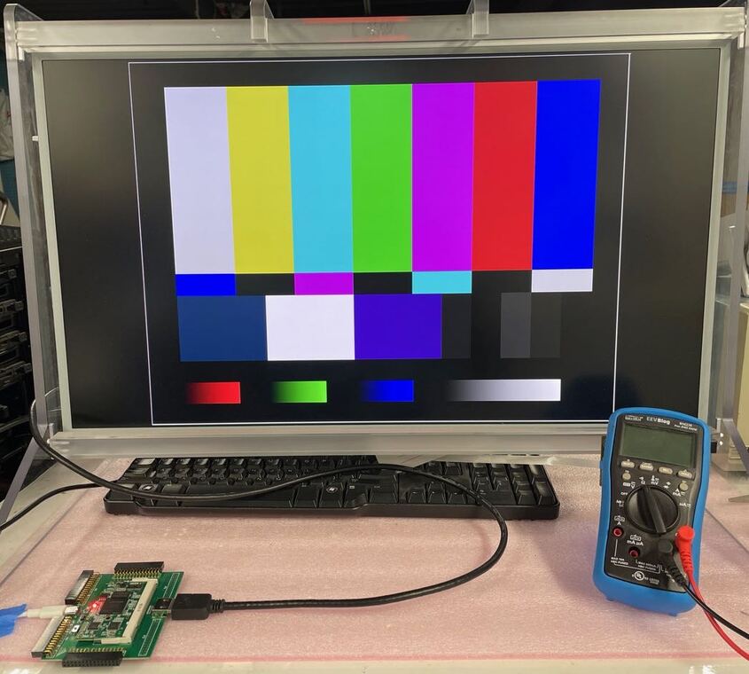
hdmi_dvi.bit
This bitstream sends a 640x480/60Hz test image to the HDMI connector.
litex_with_dram.bit
Litex is a powerful SOC RTL builder.
The litex_with_dram.bit bitstream contains a VexRiscv RISC-V CPU,
an SDRAM controller, and some kind of BIOS to boot a secondary image over Ethernet or
over the serial port.
Load the bitstream:
$ ecpdap program --freq 5000 litex_with_dram.bit
 Programming [========================================] 688.69KB/688.69KB (26.78KB/s; 0s)
Finished in 25.78s
The provided bitstream has the UART programmed at 38400 bps.
Start a serial terminal:
$ picocom -b 38400 /dev/ttyACM0
picocom v2.2

port is        : /dev/ttyACM0
flowcontrol    : none
baudrate is    : 38400
parity is      : none
databits are   : 8
stopbits are   : 1
escape is      : C-a
local echo is  : no
noinit is      : no
noreset is     : no
nolock is      : no
send_cmd is    : sz -vv
receive_cmd is : rz -vv -E
imap is        :
omap is        :
emap is        : crcrlf,delbs,

Type [C-a] [C-h] to see available commands

Terminal ready
Network boot failed.
No boot medium found

--============= Console ================--

litex>
Where you’ll catch the Litex BIOS messages will depend on how fast you started the terminal after
loading the bitstream. But at some point, you should see the litex> prompt.
If you want to see the full boot sequence, either start picocom in a different terminal window before
loading the bitstream, or enter reboot at the prompt.
I did the latter, and was greeted with the following:
litex> reboot


        __   _ __      _  __
       / /  (_) /____ | |/_/
      / /__/ / __/ -_)>  <
     /____/_/\__/\__/_/|_|
   Build your hardware, easily!

 (c) Copyright 2012-2020 Enjoy-Digital
 (c) Copyright 2007-2015 M-Labs

 BIOS built on Oct  2 2020 22:57:04
 BIOS CRC passed (5d238c53)

 Migen git sha1: 7bc4eb1
 LiteX git sha1: 8bdf6941

--=============== SoC ==================--
CPU:       VexRiscv @ 198MHz
BUS:       WISHBONE 32-bit @ 4GiB
CSR:       8-bit data
ROM:       32KiB
SRAM:      8KiB
L2:        32KiB
MAIN-RAM:  4096KiB

--========== Initialization ============--
Ethernet init...
Initializing DRAM @0x40000000...
SDRAM now under software control
SDRAM now under hardware control
Memtest at 0x40000000...
[########################################]
[########################################]
Memtest OK
Memspeed at 0x40000000...
Writes: 461 Mbps
Reads:  382 Mbps

--============== Boot ==================--
Booting from serial...
Press Q or ESC to abort boot completely.
sL5DdSMmkekro
             Timeout
Booting from network...
Local IP : 192.168.1.50
Remote IP: 192.168.1.100
Booting from boot.json...
Booting from boot.bin...
Copying boot.bin to 0x40000000...
Network boot failed.
No boot medium found

--============= Console ================--

litex>
Litex itself is worth a few articles, but out of scope for this getting started blog post.
What’s important here is that the bitstream allows you to check the DRAM is working, and to verify that the UART pipeline from PC to FPGA is functional.
Hint: Press [CTRL-A] [CTRL-A] to exit picocom.
From Verilog to Bitstream
Finally, after playing around with prebaked bitstreams, it’s time to compile our own.
If you’re lucky and don’t run into compilation issues, the process is pretty straightforward.
Step 1: Install the tools
You need Yosys, Project Trellis, and NextPnR-ECP5 to go from verilog to bitstream.
-
Compile and/or install Yosys
Most Linux distributions come with a Yosys package, but since Yosys is moving quickly, I recommend compiling it from scratch.
You can find instruction here.
-
Compile and/or install Project Trellis
Project Trellis is name of the effort by David Shah to reverse engineer the internals of the Lattice ECP5 FPGA family. This work is what allowed all of us to use ECP5 in a full open source flow.
You can find it in the prjtrellis GitHub repo.
I personally prefer to install
prjtrellisin the/optdirectory instead of the more common/usr/libenvironment. When you do so, make sure thatnextpnr-ecp5, the place and route tool, knows about this location as well.If you want to do the same, follow the project installation instructions, but run
cmakewith these parameters:cmake -DCMAKE_INSTALL_PREFIX=/opt/prjtrellis . -
Compile and/or intall NextPnR
NextPnR takes a synthesized netlist from Yosys and performs the place-and-route operation of the netlist into the FPGA.
You need to build a version of NextPnR that is specific to a particular FPGA family. In this case, we’ll be building
nextpnr-ecp5.The installation instructions are here.
Like
prjtrellis, I prefernextpnr-ecp5to be installed in its own/opt/directory, so I changed thecmakecommand line parameters as follows:cmake . -DARCH=ecp5 -DTRELLIS_INSTALL_PREFIX=/opt/prjtrellis/ -DCMAKE_INSTALL_PREFIX=/opt/nextpnr-ecp5Note: on my main Ubuntu 18.04 machine, I couldn’t compile
nextprn, due to some weird issue with not finding thepthreadlibrary. On my Ubuntu 18.04 laptop, things worked without issue. -
Make sure that Yosys, Project Trellis, and NextPnR are in your
$PATHIn my case, I had to add this to
~/.profile:PATH="$PATH:/opt/nextpnr-ecp5/bin:/opt/prjtrellis/bin"Yosys was installed under
/usr/local/, which was already in my$PATH.
Step 2: Compile a project
Let’s compile the blinky project:
cd Colorlight-FPGA-Projects/src/i5/blink/
make clean
make
If all went well, you’ll see a lot of text scrolling over the screen, which will end with something like this:
...
Info: [ 36103,  37397) |****************
Info: [ 37397,  38691) |*************
ecppack --svf blink.svf blink_out.config blink.bit
You will also find a new blink.bit file waiting for you. Load to the FPGA with ecpdap as explained earlier.
Congratulations! You’ve cleaned the pipe from Verilog all the way to a working FPGA design!
Using the Board for Your Own Projects
It’s one thing to compile an existing project, it’s another to create one yourself. As a test, I ported my SPDIF PMOD design from an Intel MAX10 to this development board.
The Colorlight i5 specific changes were minimal.
Some miscellaneous findings:
-
Lack of SODIMM/connector information
The information is all there to make things work, but it’s more of a hassle than needed.
Here’s an example: if you want to assign the pins of a PMOD on connector P6 to an FPGA pin, you need to take the following steps tracing through the board schematic:
-
map pin 2 of your PMOD to pin 26 of connector P6.
There is some guess work involved here, because it could just as well be pin 5 on connector P6.
-
check that pin 26 is connected to net PL38A.
PL38A happens to be the name of the IO pad of the FPGA silicon, but that’s NOT the same as the FPGA package pin name.
-
look up that net PL38A aliases to net M4, connected to pin 72 of the SODIMM connector, which happens to be the FPGA package pin name.
This gets tedious quickly.
This issue can easily be solved with a few more tables in the documentation.
I created my own FPGA pin to connector mapping diagram. You can find it here
-
-
Limited FPGA PLL support
This is a limitation of the ECP5 open source flow.
Project Trellis has the
ecppllutility to generate PLL models. It works fine in simple mode, but that has only very limited clock resolution: I wanted to generate a clock of 12.288MHz out of the 25MHz oscillator, but only got 12.5MHz.ecppllhas the--hiresoption which is supposed to increase the resolution, but when I used the generated PLL for that, nextprn errored out. (Issue filed.) -
Use bitstream compression to improve bitstream loading times
Like most modern FPGAs, the ECP5 supports bitstream compression. This significantly reduces the size of the bitstream, especially for smaller designs, and improves load times from PC into the FPGA.
For example, on my SPDIF example, which is very small, it reduces the bitstream from 582KB down to just 100KB.
There are 2 ways to enable bitstream compression:
- use
--compressas command line parameter of theecppacktool - add
SYSCONFIG COMPRESS_CONFIG=ON;to the project lpf file.
- use
-
Fantastic compile/place & route turn around time
On my Intel Max10 development kit, it takes 33s to compile from Verilog to bitstream. With Yosys/NextPnR, that same design takes 2.5s!!!
On the other hand, loading the bitstream with Quartus takes only 1 second, compared to 4s for the Colorlight i5 (after enabling bitstream compression.)
It’s still a major win for the Colorlight and the open source flow.
Conclusion
I really like the Colorlight i5 + development board combo. The FPGA is large enough for interesting projects, it’s perfect if all you need is an FPGA, DRAM, and a lot of IOs. It’s supported by open source tools. The HDMI output is a nice bonus. And, most of all, at $50, it’s cheaper than anything else in its class.
The only negatives are documentation that’s lacking, and the absence of interfaces like Ethernet, SDcard, etc. If you want those, you’ll need to add expansion PMODs, or you can switch to a ULX3S development board… at a significantly higher price.
References
- Colorlight i5 Product Page
- Item on AliExpress
- Official Development Board GitHub Repo
- Colorlight i5 Tips GitHub Repo
- Using ColorLight FPGA board with cheap JTAG programmers
Similar FPGA boards
(Thanks pauluzs!)
-
Another board by Muse Lab that uses the same expansion board, and also ECP5-LFE5U025F FPGA, though with a different package. Features are similar, though there are no Ethernet PHYs
-
Uses a Lattice ECP3-LFE3-35EA-6FN484C, and not supported by any open source tools. I’m not aware of a reverse engineering effort.
-
Uses a Lattice ECP5-LFE5U-45F-6BG381C.
-
Uses a Xilinx XC7AA50T-FGG484ABX1909.
-
Uses a Xilinx XC6SLX16-CSG324DIV1645.
Extension Boards
-
Colorlight Dual Ethernet Board
Sold second hand by Muse Lab, this adds the IOs for 2 Ethernet ports as well as connectors to drive LED matrices. The IOs are all buffered and thus output only!