Reverse Engineering the Comtech AHA363 PCIe Gzip Accelerator Board
All this work was done in November last year. I haven’t worked on it since, but others have shown interest in picking this up, so it’s about time this gets thrown out in the open.
- The Start of a Journey
- Undressing the FPGA
- AHA363 Board Overview
- Probing, Test points, and Tented Vias
- Package Footprints and Intel Quartus
- Correlating FPGA IOs with the FPGA vias on the PCB
- The JTAG Connector
- Scanning the JTAG Scan Chain
- Saving the Parallel Flash Contents
- Reprogramming the Parallel Flash File
- Powering from the Bench
- The Problem of Loading a New Serial Bitstream
- Decoding a POF file and Creating a New One
- End of Part 1
- References
The Start of a Journey
One can never have enough projects going in parallel. And while programming RTL is fun, I also love the whole process of reverse engineering, starting from a board that you don’t know nothing about and step-by-step getting to the point where it becomes something useful.
The FPGA board hack project on Hackaday lists a bunch of commercially available PCBs that have an FPGA in them. Most of them haven’t really been comprehesively reverse engineered.
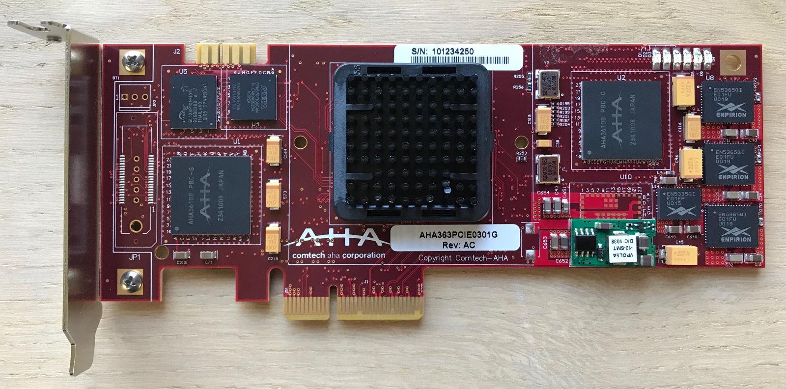
FPGA development boards with PCIe support are never cheap, so I was particularly attracted to the Comtech AHA363PCIE0301G (AHA363). It’d be fantastic if it could be repurposed as a general FPGA PCIe accelerator board.
The AHA363 is listed as having an Arria GX FPGA, size unknown. Its real purpose is a gzip compression and decompression accelerator, a common operation in data centers that need to serve gzip compressed web pages.
Various eBay vendors sell the same board for wildly differing prices: $1265, $185, and $19. In an attempt to keep my wife happy, I settled on the $19 version. Or better: I bought 2 of them, in case I needed to destroy one to figure out connections etc.

In this blog post, I’m describing the journey from acquiring the board to getting to the point of doing something useful with it. There is no guarantee of success: at the time of writing this, I haven’t been able to get an LED to blink yet, but I’ve already learned some new techniques that will help me reverse engineer other PCBs in the future, and that might be useful for others as well.
A few days after ordering, this arrived at my doorstep:
Undressing the FPGA
Note: for those who’d like to replicate/help out with reverse engineering this thing: now that we know the type of the FPGA, there’s really no reason to remove the heatsink anymore. This reduces the chances of accidentally destroying your board.
The FPGA Board Hack project mentioned an Arria GX FPGA, but since it’s covered by a heat sink, the exact type was still unknown.
The heat sink is mounted solidly to the chip with 2 clips on 2 sides. You can remove it by inserting a flat head screwdriver in the clip holes and pushing them out. After a bit of wiggling, the mounting bracket will come off. Next, squeeze the same flat head screwdriver between the FPGA and sink, and rotate it very gently separate them. Eventually, the sink will come off, and the secret is revealed:
What we have here is an Arria GX EP1AGX90E: the largest device of its class with 90K logic elements, 4.4Mbits of block RAM, and 176 18x18 multipliers. Even today, boards with FPGAs of this size are in the ~$100 range.
Reverse engineering this project got a lot more interesting!
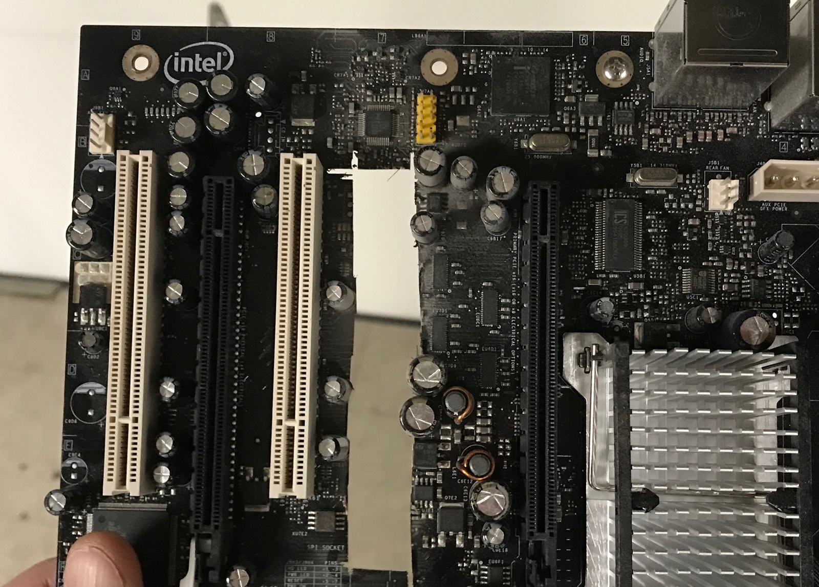
AHA363 Board Overview
The PCB of the AHA363 is packed with a large number of ASICs and components. It’s a half-height 4x PCIe board with a bracket of the same height: that’s fine for a rack-mounted server, but it won’t fit inside a regular PC. You need to remove that bracket first.
After doing that and plopping the board (with the heat sink!) into my regular Linux PC, lspci greeted
me with the following message:
XXX To be added XXX
Success! The board is working!
The first step of my reverse engineering process is to take photographs at close range of all the components and connectors. In most cases, the x2 optical zoom option of my iPhone 7 Plus is sufficient for that, but sometimes I use the iPhone adapter on my microscope. My eye sight has been declining, and photos make it so much easier to identify the markings of various components.
I also annotate these photos with the component names, connector pins values etc. This makes it much easier when needing to find your bearings when probing things.
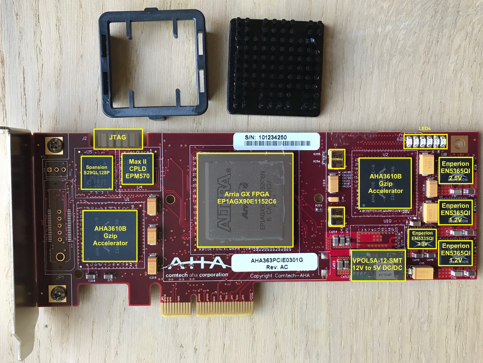
The PCB contains:
- 1 Intel Arria GX EP1AGX90E FPGA
-
2 AHA3610 gzip accelerator ASICs
Other than some slide sets and marketing material, I could not find any technical datasheets about it.
-
1 Spansion S29GL128P parallel flash
Contains the FPGA bitstream that gets loaded in the FPGA at boot-up.
It’s common for FPGA-based PCIe card to have parallel flash instead of the more commonly used serial flash: parallel flash not only loads faster, but it also support multiple bitstream images in the same flash and selecting between them. Intel FPGAs don’t support that with serial flash.
-
1 Altera MAX II EPM570F100 CPLD
Used to copy the bitstream from flash into the main FPGA. This CPLD is used in the same configuration in the Altera Arria GX development kit, and in the reference designs for remote system upgrade designs.
-
a 10-pin connector
Almost certainly as JTAG conector. Maybe more?
-
1 VPOL5A-12-SMT 12V to 5V DC/DC convertor
This is probably the DC/DC convertor to bring down the PCIe supplied 12V to some rough regulated 5V, with other regulators doing the more detailed work.
- 4 Enperion Power Convertors
- 2x 6A EN5365QI for 1.2V
- 1x 6A EN5365QI for 2.5V
- 1x 3A EN5335QI for 3.3V
-
2 100MHz Xtal Oscillators
Why two?
-
6 LEDs
Absolutely essential if we want to get an LED blink working on this board!
-
PCIe interface
The head attraction of this PCB and the main reason why it gets reverse engineered!
One immediately notices that this board get pretty warm when plugged into the PC, even when it’s not doing anything useful.
Probing, Test points, and Tented Vias
The most important tool for reverse engineering a PCB are a multi-meter with a low reaction time when using it in short-detect mode. This makes it possible to go over an array of vias very quickly in the hope to triggering a connection between 2 points.
Another key element is the ability to measure connections in the first place: if you’re really lucky, the PCB has plenty of test points. If you’re a bit lucky, there are tons of vias that are not tented. You’re totally out of luck if your doesn’t have test points and vias are tented at all. In those cases, I usually bail on the whole reverse engineering thing: discovering connections becomes simply too cumbersome.
The Pano Logic G2 has motherboard PCB doesn’t have tented vias. You can see accessible blank copper around each via hole.
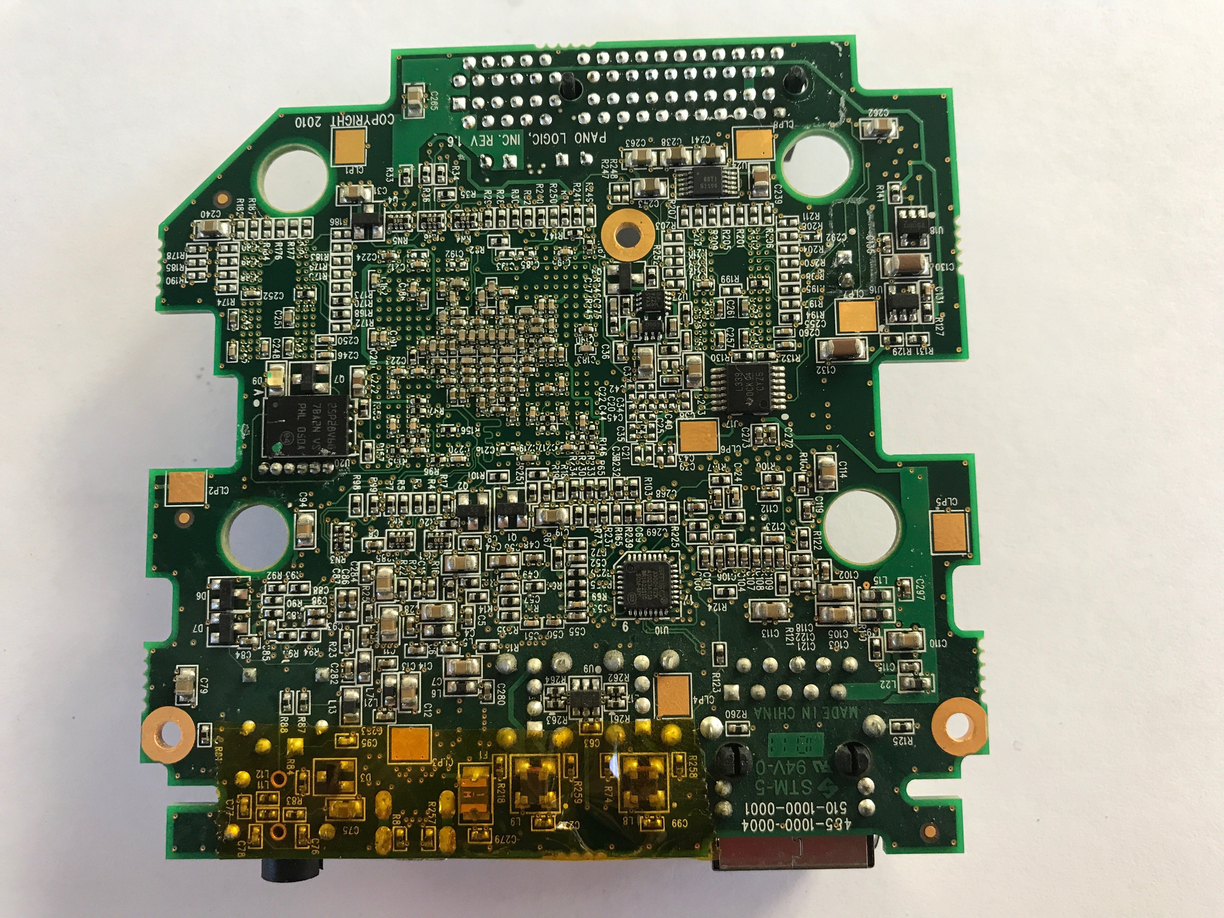
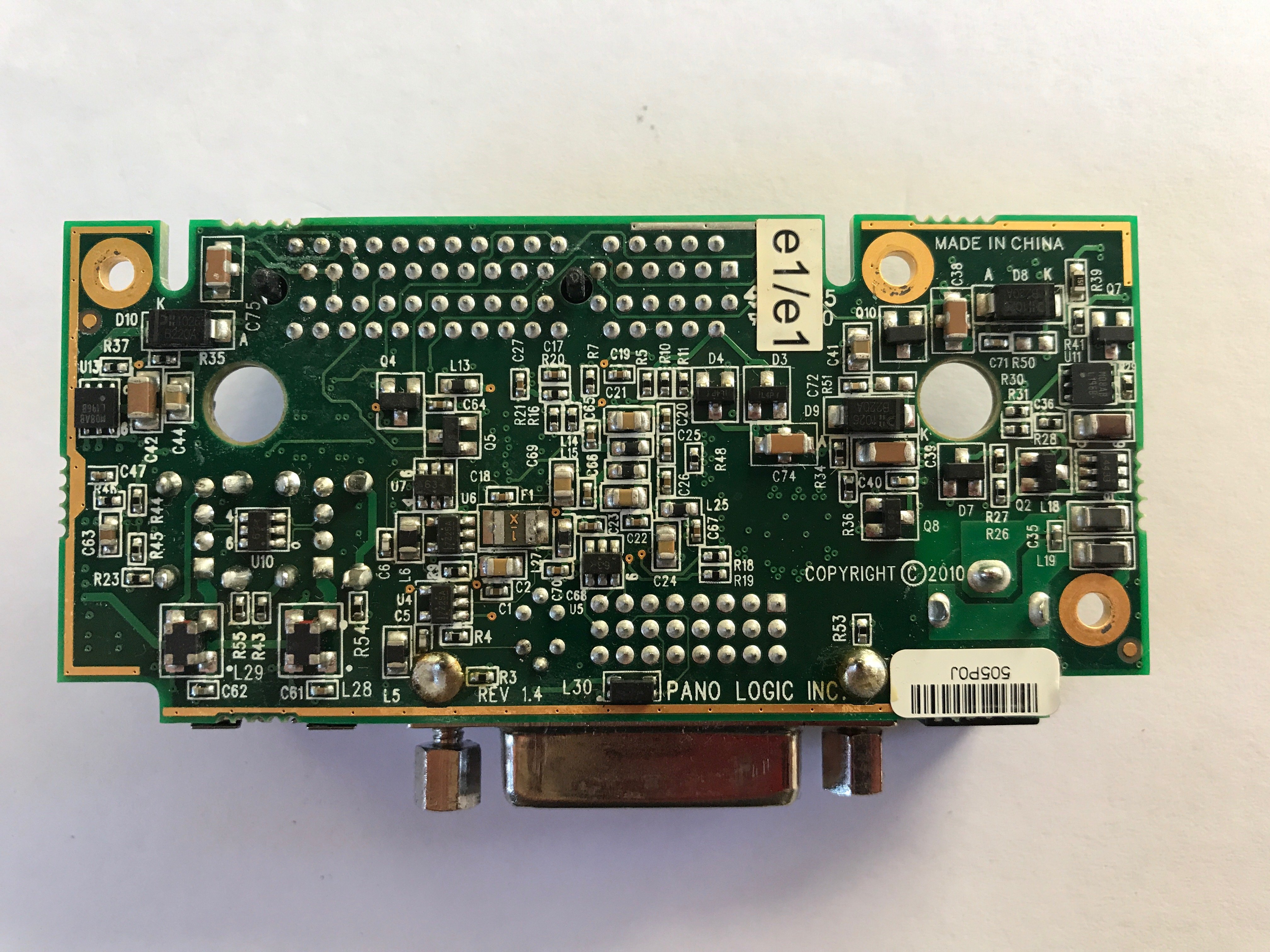
However, the Pano Logic G2 auxiliary board has a number of accessible test points, but the remaining vias have their copper covered:
The AHA363 board has an incredibly amount of test points, more than I’ve ever seen before. So that’s fantastic. But strangely enough, one of my boards had tented vias and the other did not. I’m using the one with tented vias to record traces with my scope and logic analyzer to check dynamic behavior, and I’m using the other board to probe out connections.
That said, pressing the sharp tip of my oscilloscope’s probes on the tented vias is usually sufficient to break through the protective layer and make it peel off a little bit. After that, those vias can be probed without much difficulty.
Package Footprints and Intel Quartus
The Arria GX product family is pretty old now, and not supported anymore by today’s versions of Quartus. The last official release with support was Quartus 13.0sp1, but that was only for the standard, commercial version. The last ‘free’ release was Quartus 11.0. You can download it here.
I’ll use Quartus for a number of reasons:
- Quartus Programmer is very good at discovering all the JTAG TAPs (test access ports)
- We’ll use Quartus to create new bitstreams for our design.
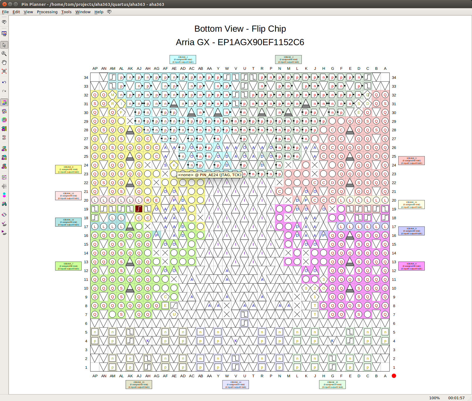
- The Quartus Pin Assignment editor gives an excellent view of the IO pins of the package, with the ability to view the package from the top or bottem, and at any desired rotation. This is a life saver when trying to find pinpoint the right IO pad on the PCB. The assignment editor also annotated all the special IO pads with the right value when you mouse over it.
Here’s a screenshot of the Pin Assignment Editor showing the Arria GX FPGA as seen from the bottom of the PCB, with the PCIe transceivers located at the bottom too.
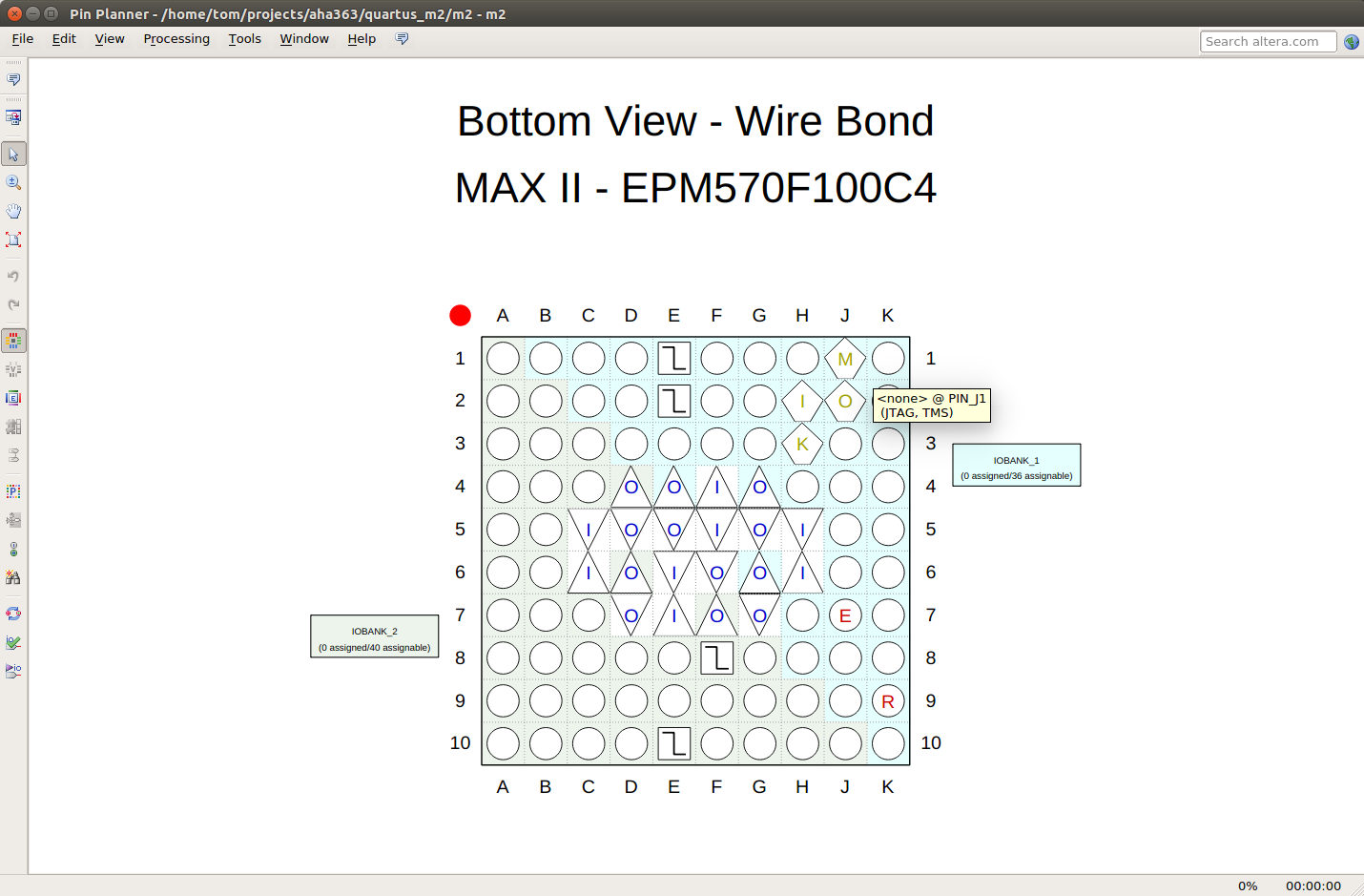
And here’s the MAX II CPLD:
Correlating FPGA IOs with the FPGA vias on the PCB
When you’re lucky again, the PCB has vias underneath the FPGA that map directly to the balls on the FPGA package.
When your PCB doesn’t have this, you may be forced to desolder the FPGA of one of your boards at one point or another.
In the case of the AHA363, there is a pretty decent grid of vias underneath the FPGA, but it’s still a bit of a struggle to find the correlation between the vias and the ball on the package.
Time to bring out an image editor (I use Inkscape because it works both on the Linux PC in my lab and on my Mac) and start annotating the vias with the most plausible pad name. This is not always the linear process that’s describe here: I first located some JTAG pins (see next step), then annotated those pins, then located some the clock (see down even further), annotated those etc.
Eventually, I ended up with something like this:
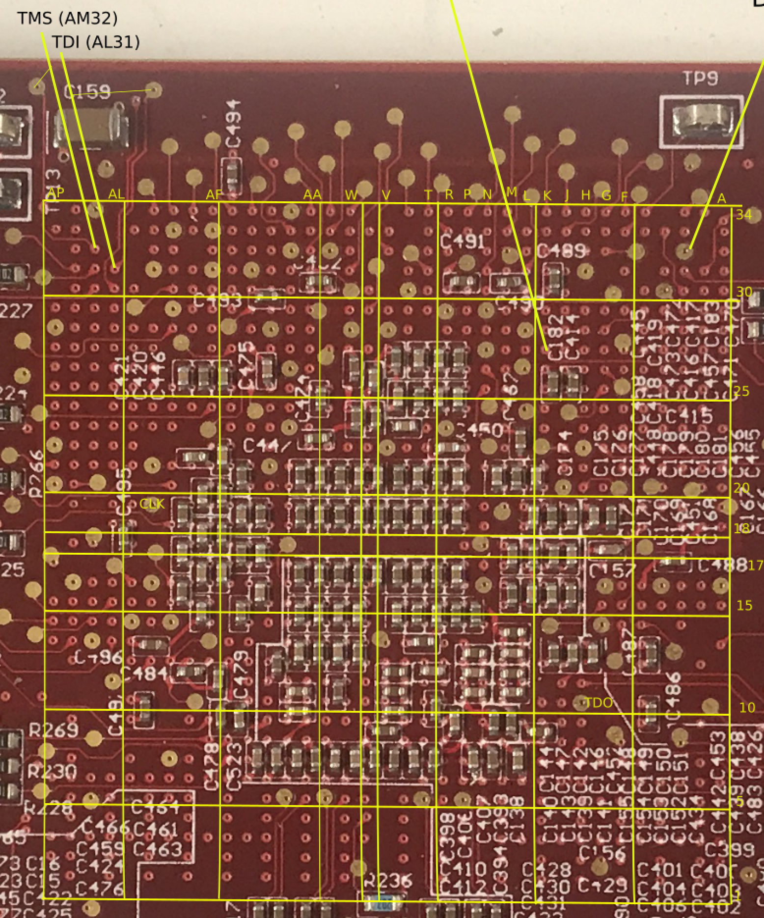
The column and row annotations are at the top and the left. I add grid lines every 5 BGA balls.
Notice how there’s an extra column of balls between columns V and W and and an extra row of balls between rows 17 and 18. This has been the case for all PCBs that I’ve dealt with: the vias don’t coincide with the balls on the BGA, but they fall right in between, so there’s always an extra row or column right down the middle.
The JTAG Connector
Nothing is more important while reverse engineering an FPGA-based PCB than getting the JTAG interface to work, since it’s the prime method of loading bitstreams during FPGA development. In addition, FPGAs also have boundary scan registers for most IO pads that make it possible to extract sometimes crucial additional information about how IOs are configured (input or output), locate the clocks, and the values that are being driven or that are being read by the IOs.
Many FPGA based PCBs have their JTAG interface easily available, even on the final production board, since it’s often used as the main interface to program production firmware and bitstreams on the factory production line.
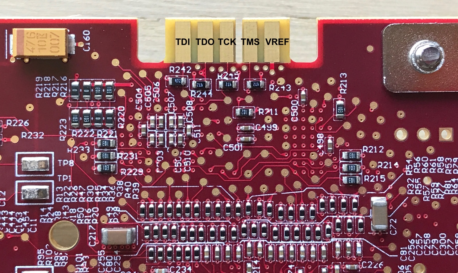
The AHA363 has a prominent 10-pin connector that I expected to contain JTAGs pins, so the next step is to figure out how those pins are connected.
- 4 of the 10 pins are connected to ground. They are all on the front (component) side of the PCB.
- on visual inspection, the remaining pin on the front side seemed to be unconnected (since there was no via from the connector metal to anywhere.)
- that leaves 5 more pins: TCK, TMS, TDI, TDO, and VREF. VREF is the IO supply voltage that goes from the PCB to the voltage level shifters in the JTAG dongle.
The discovery process is pretty straight forward: you start with one of the JTAG pins that is shared between all chips in the chain, TCK or TMS. You check if there’s a connection between those IO pads on the FPGA and one of the connector pins. Done!
I was able to identify TCK and TMS quickly, but had no such luck for TDI and TDO.
The thing is that TDI and TDO are point-to-point, and they can be part of a chain. If the FPGA is in the middle of a JTAG chain, then these pins on the FPGA package will not be connected to the connector.
So the next step is to check the TDI pin of the CPLD, and bingo: it goes straight to the JTAG connector!
I also confirmed that the TDO pin of the CPLD is connected to the TDI pin of the FPGA.
Since there is no connection between the FPGA TDO and the connector, it’s likely that the 2 ASICs are part of the JTAG chain as well. We don’t know anything of their pin-out, so that’s a dead-end.
But if one of the pins is VREF, you can try checking if there’s a connection between one of the 2 pins and VDD. And, indeed, there is! And since there’s now only unknown left, that one can be assigned to TDO.
Scanning the JTAG Scan Chain
With the JTAG connector figured out, the next step is to get the scan chain working.
That’s obviously only possible when the board is powered up, but a PCIe card can have a potentially complex power supply architecture: the PCIe connector has 12V, 3.3V and 3.3Vaux pins, and it’s not yet clear which ones are used by this board.
Luckily, instead of powering the board on a lab bench, there’s a much simpler way: you plug it into a working machine! As luck would have it, I was able to save a very old Mac Pro from the dumpster and other than being slow, it just works.
I soldered some wires from the AHA363 JTAG pins to a 10-pin connector with Intel USB-Blaster arrangement and ended up with this:
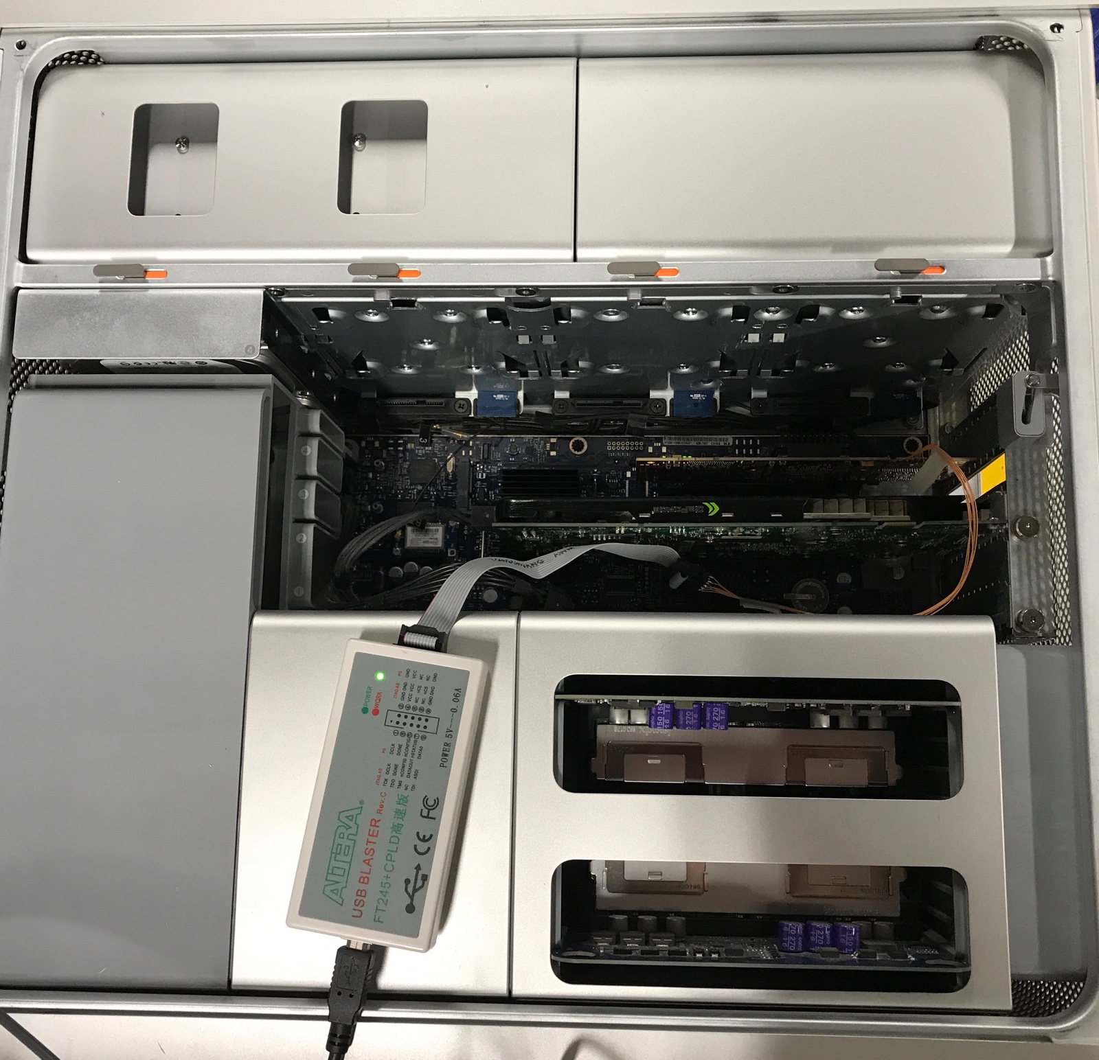
The Mac was able to boot up fine (and ignored the AHA363 as expected).
I fired up Quartus Programmer, and after pressing “Auto Detect”, I was greeted with the following:
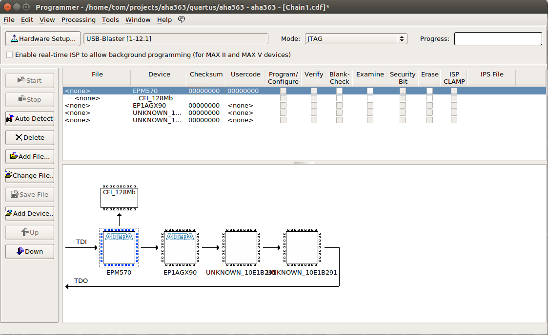
Success!
As expected, the 2 AHA363 are part of the JTAG chain. This will soon give me major problems…
Saving the Parallel Flash Contents
In the previous image, you can see how the Max-II CPLD has the 128Mbit parallel flash connected to it.
We’re probably going to messing around with the contents of the flash by programming a new bitstream into it, so now is a good time to make a backup of that.
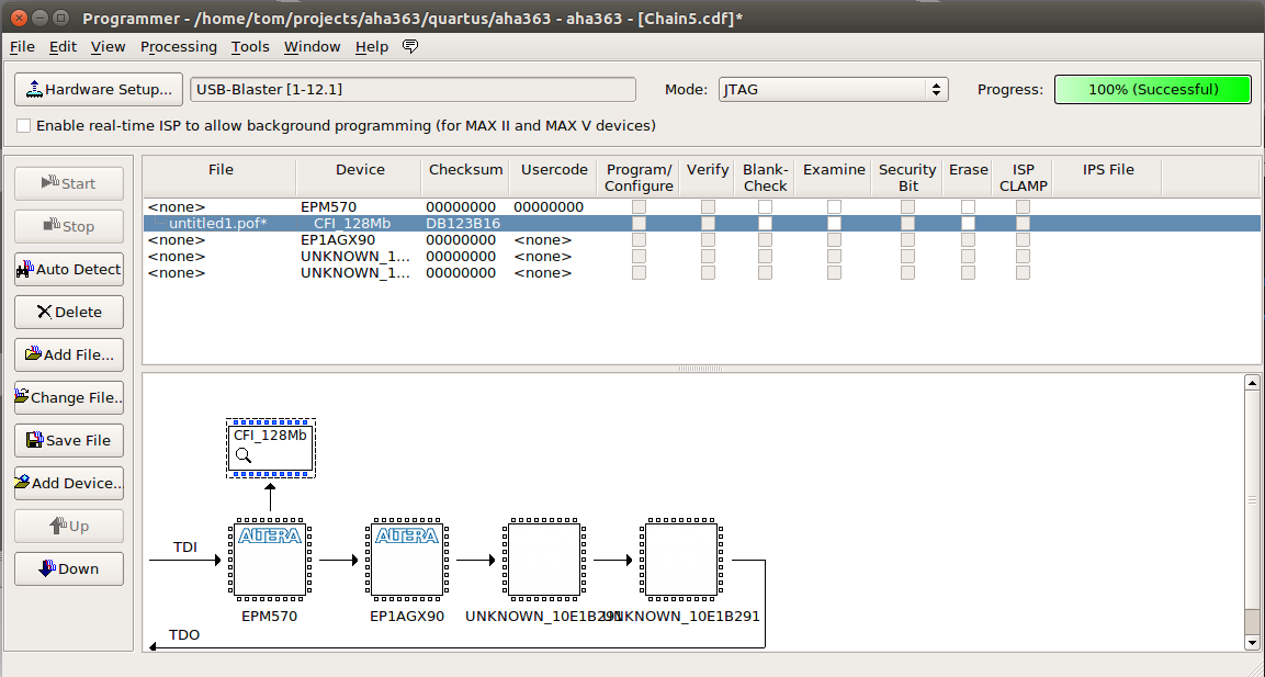
In Quartus Programmer, select the “Examine” flag next to “CFI_128Mb” and press the “Start” button.
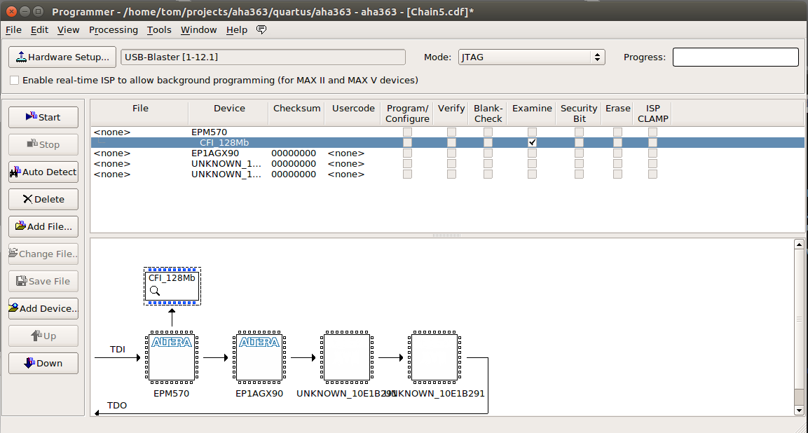
Now right click on untitled1.pof and do “save File”.
Reprogramming the Parallel Flash File
You won’t need this yet, but to reprogram the flash:
-
First Erase the flash memory
CFG_128Mb -> Erase -> Start -
Reprogram the flash file
CFG_128Mb -> Right click: Change File (NOT Add File!!!) -> Select .pof file -> Start
Powering from the Bench
It’s really hard to reverse engineer a board when it’s sitting inside a PC enclosure!
The next step is to detect the JTAG chain while the board is sitting alone on the bench.
We know that that power comes in through the PCIe connector, so we could solder some wire on there. But we also want to be able to still plug in the board into a working PC.
Wouldn’t it be great if we had a female PCIe connector?
Well… I didn’t have that in my parts kit, but I did have an old, broken motherboard! A few minutes of Dremel action later, I had this:
And a short PCIe connector!
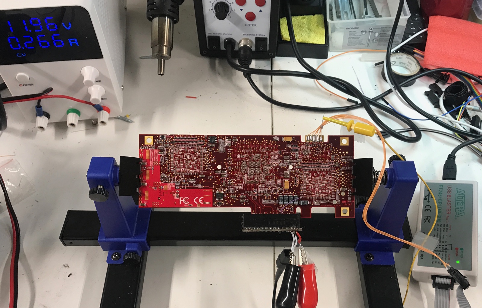
I was lucky with the power supply situation: the 3.3V and 3.3Vaux pins of the PCIe connector aren’t going anywhere on the PCB, so the whole PCB is only powered by the 12V.
So all I had to do was wire up 12V pins on the female PCIe connector.
And once powered up, the JTAG chain was still working fine!
The Problem of Loading a New Serial Bitstream
When reverse engineering an FPGA board, creating tiny designs to verify assumptions about pinout and then loading that bitstream into the FPGA through JTAG is essential.
This normally happens by shifting in a so-called SOF file.
But remember how the JTAG scan chain contains 4 devices: a Max-II CPLD, the Arria GX that we’re interested in, and the 2 AHA363 chips.
One way or the other, I was not able to load an SOF file into the FPGA. The SOF would shift in correctly, but soon after the FPGA would receive a reset from the CPLD. I tried forever to make it work and it just didn’t…
Decoding a POF file and Creating a New One
The alternative is to reprogram the parallel flash of the FPGA with the desired bitstream. But for that, you need to know the layout of this parallel flash.
The POF files contains multiple segments with different kinds of information. If you know the contents of these segments, you can create a new POF file yourself and load that into the FPGA.
The problem was how to get that information out of a POF file?
I found a document online that describes the POF file format! It’s only 2 pages, and refers to the original Altera MAX CPLD devices, so it’s probably more than 20 years old. But it’s better than nothing.
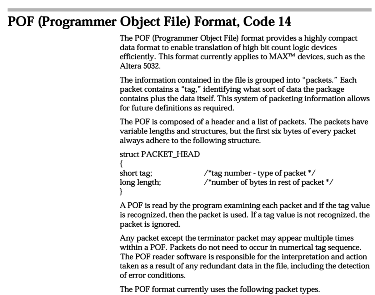
With that information, I could write a POF disassembly tool.
When I execute this tool on the bitstream that I dumped from the board earlier, I get a file with all the different chunks.
But most important piece of information is this:
==============================
Tag: 26 (Flash Chunks <unofficial>)
Length: 124 (0x0000007c)
Field 0: 0x00ff0000 (16711680)
Field 1: 0x03800000 (58720256)
Field 2: 0x00010000 (65536)
Content:
mCFI_128Mb 00000000 08000000
mPage_0 00000000 00D90000
mPage_1 00800000 00D90000
oOPTION_BITS 00FF0000 00000408
This shows where major pieces of the POF file are located.
Armed with that information, I was able to create
a .cof file: a configuration
file for the Quartus Convert Programming File tool that is used to convert a .sof file into a .pof file.
I was now able to flash a new bitstream info the parallel flash! A major success!
End of Part 1
Unfortunately, it didn’t get me anywhere interesting: as soon as I load some new bitstream the board refuses to work. I suspect that some FPGA IOs are controlling the voltage regulators on the board, and my code is clearly not doing that.
I’m only able to recover the board back by plugging it into the Mac Pro and then reflashing the original firmware.
There are other ways to proceed though: you can use JTAG to dump the direction of all FPGA IOs, the value that these are IOs are driving or the value that they are receiving.
That’s the subject of another post.