Pano Logic G1: Works Have Started
After transcribing the data from previous reverse engineering efforts , and an insane amount of effort to Xilinx ISE 14.7 to work with my Digilent JTAG clone, I’ve started for real with the mapping out the pins of the FPGA.
The PCB is remarkable in that all the balls of the FPGA and the SDRAM BGAs have an accessible via.
That makes it really easy to figure out all the connections between them. So that’s the work that got completed first.
The remainder of the chips are some form of a QFP. You can figure out the connections either by installing a ChipScope (similar to how I did some of the eeColor Color3 pins), but that doesn’t work for inputs to the FPGA.
It’d be much easier to remove the FPGA from the board and Ohm things out that way.
But that’d be a deliberate act of violence and destroy the board.
Well… I bought a lot of 5 of them for $45.
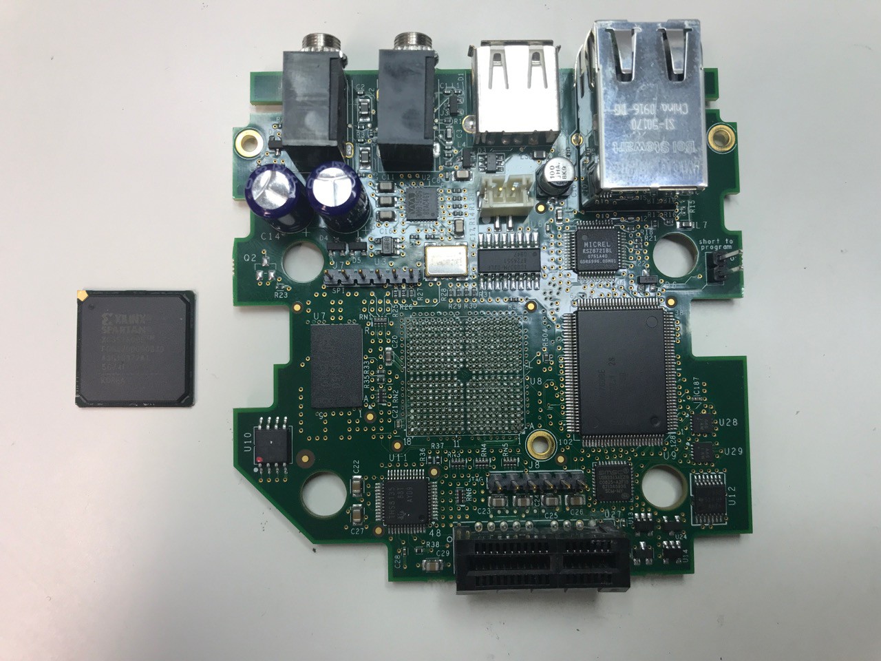
So off when the FPGA. Feel dirty, man.
I’ve now mapped out the full connection between the FPGA and the TI VGA Out chip. At this point, this should enable me to send an image to a monitor, but VGA is so old now that I couldn’t find a VGA cable at home (or even at work.)
While waiting for a cable, I’ve started mapping out the USB host chip as well.