The HP 423A and a Beginner's Deep Dive into RF Crystal Detectors
- Introduction
- What is a Crystal Detector?
- Diode Square Law Behavior
- The HP 423A Crystal Detector
- The Crystal Detector in Action
- Playing with the Detector Load
- Why Do We Want Square Law Behavior Anyway?
- Why Does the Load Resistor Shift the Square Law Region?
- Power Measurement with Crystal Detectors
- References
- Footnotes
Introduction
I picked up some random RF gizmos at the
Silicon Valley Electronics Flea Market.
It’s part of the grand plan to elevate my RF knowledge from near zero to beginner level: buy
stuff, read about it, play with it, spend more money, hope to learn useful things.
I’ve found the playing part to be a crucial step in the whole process. Things seem to stick
much better in my brain when all is said and done.1
In this blog post, I’m taking a closer look at this contraption:
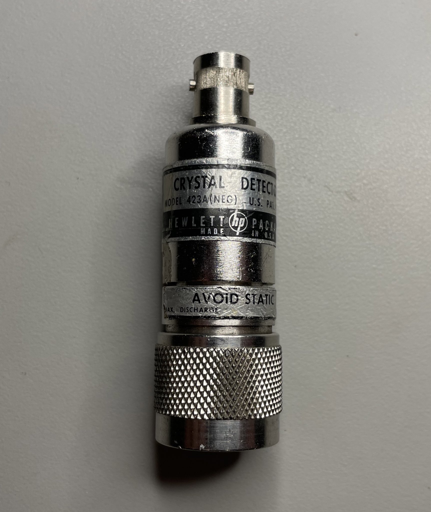
It’s an HP 423A crystal detector. According to the operating and service manual:
[the 423A crystal detector] is a 50Ω device designed for measurement use in coaxial systems. The instrument converts RF power levels applied to the 50Ω input connector into proportional values of DC voltage. … The frequency range of the 423A is 10MHz to 12.4GHz.
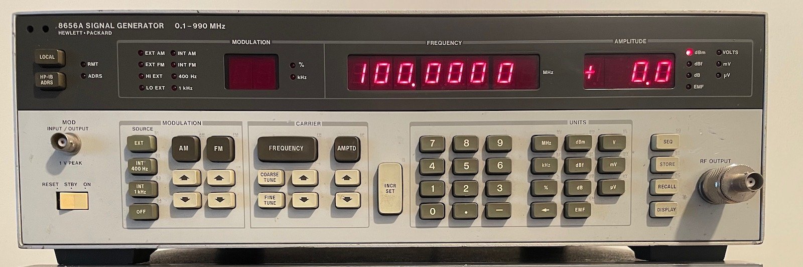
At last year’s flea market, I picked up a dirt cheap, and smelly, HP 8656A 990MHz signal generator. It has support for amplitude modulation which is what I needed to give the detector a good workout.
In the process of playing with the detector, I discovered some warts of the signal generator, I picked up an RF power meter on Craigslist, learned a truckload about RF power measurements and the general behavior of diodes and the math behind it, I finally installed ngspice and ran a bunch of simulations, and figured out a misunderstanding about standing-wave ratio (SWR) and their relationship with crystal detectors. (Phew)
In this blog post, I’m covering some of the theory being crystal detector, I’lll do a bunch of measurements, and I’ll have a look at some applications.
What is a Crystal Detector?
So what exactly is a crystal detector? Wikipedia claims that…
… a crystal detector is an obsolete electronic component used in some early 20th century radio receivers that consists of a piece of crystalline mineral which rectifies the alternating current radio signal.
If they are obsolete, then why are plenty of companies still selling them? It’s because Wikipedia is refering to the original crystal detectors that started it all: diodes that were built out of crystalline minerals instead of contemporary diodes built out of silicon, germanium, etc. Those early crystalline mineral diodes were one of the first semiconductor devices.
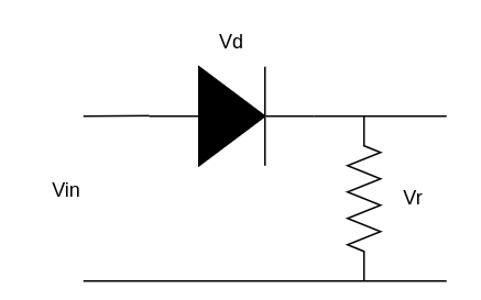
Today’s RF crystal detectors are not fundamentally different. This Infineon application note describes how RF and microwave detectors are still built with a diode, a capacitor and a load resistor. They now use low barrier Schottky diodes, but the name crystal detector stuck.
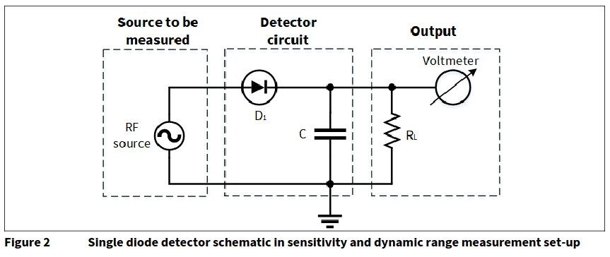
Their functionality is straightforward: the diode passes only the positive voltage of an RF signal though to the other side, a capacitor gets charged up to the peak level of the signal but discharges, slowly, due to a load resistor. If all goes well, the output voltage of the detector tracks the envelope of the RF signal.
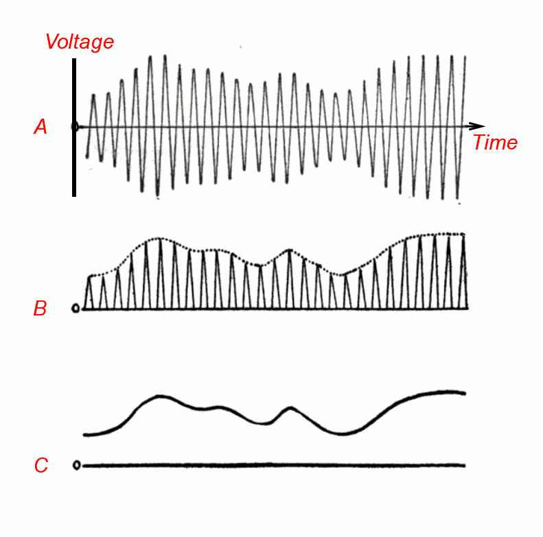
This envelope output signal is called the video signal, a bit of a confusing name because the output signal may not have anything to do with video at all, but you better get used to it because it’s a standard term in the world of RF. Even cheap spectrum analyzers, such a TinyVNA Ultra have a menu to change VBW, the video bandwidth.
In the early years, crystal detectors were used to build AM radio receivers. As a kid, I played with a RadioShack 150-in-1 kit, and one of the projects was exactly that, an AM radio crystal radio.
 (© CC BY 2.0 Caroline)
The schematic is very simple.
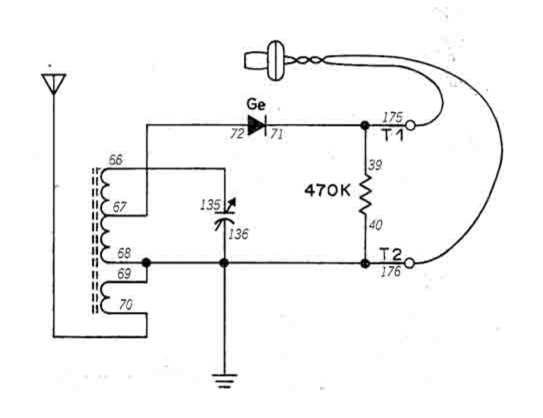
On the left, a ferrite rod antenna and a variable capacitor create a tunable LC network to select the radio frequency. A germanium diode does the detection with a 470KΩ load resistor. The schematic doesn’t have a capacitor: the output is a piezoelectric earpiece has the required capacitance. Notice the absence of a battery: the whole circuit is powered by the picked-up radio waves.
AM radios have long ago moved on from crystal detectors to better solutions. Modern demodulators mix (multiply) the incoming signal with a locally generated RF sine wave which makes the original LF signal emerge.
It’s not 100% clear to me if crystal detectors are currently still being used to demodulate other types of AM content. When you google for crystal detectors today, most hits talk about using them for RF power measurements or for power leveling, where a power measurement is part of a feedback loop that’s used to regulate the output of an RF signal source.
Here’s an example of such a power leveling setup, taken from an HP application note :
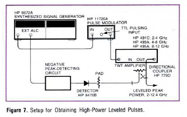
Detector HP 8470B, a close cousin of my HP 423A, measures the power of a chain that starts at a signal generator, goes through a pulse modulator, an amplifier, and a directional coupler. The output of the detector ends up back at the signal generator through its automatic level control (ALC) input.
Diode Square Law Behavior
A little bit of theory about diodes now will go a long way in understand what comes later.
A diode is often simplified to a device that blocks current when the voltage across its junction is less than a certain threshold level, and that passes current otherwise. Such an ideal device has the following voltage to current graph:
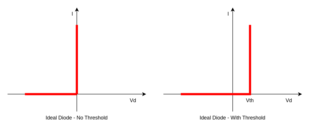
The resistance of the diode is zero above the threshold and infinite below. In practice, a diode is always used in a circuit that has some kind of some kind of series resistance (not necessarily resistor!) to limit the current. Together, the diode and this resistance form a voltage divider.
When the diode is ideal, the infinite current characteristic simply means that the voltage across the diode will always be limited to the threshold voltage, and that the remainder of the diode/resistance combo will fall over the resistance.
In reality, a diode doesn’t behave like a clean on/off device that depends on the voltage across the device. Instead, the current/voltage curve can be described with the following formula:
\[I(Vd) = \begin{cases} I_S(e^\frac{qV_d}{nkT}-1) & V_d>V_z \\ -\infty & V_d \le V_z \end{cases}\]The plot of this function looks like this:
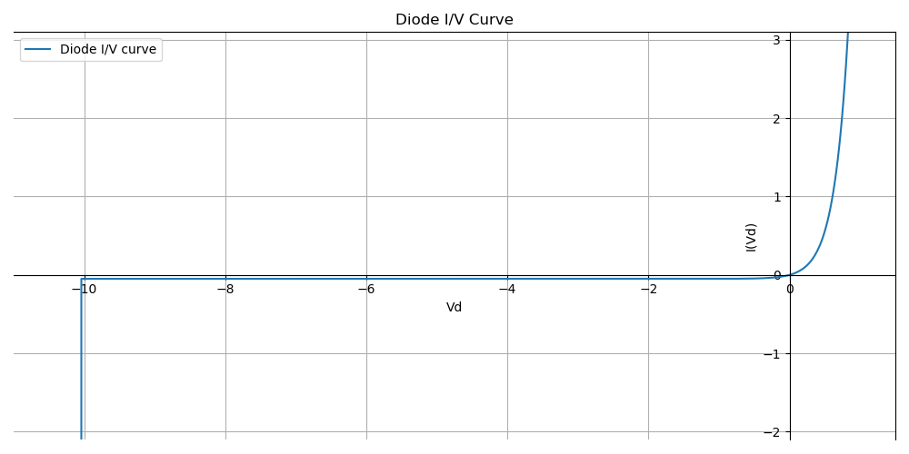
Above \(V_Z\), the reverse breakdown voltage, the curve is an exponential function. Below the reverse breakdown voltage, the diode self-destructs…
Compared to an ideal diode, there is:
- a small current when the diode is reverse polarized
- a smooth transition region to go from almost no current to a lot of current
- the reverse breakdown voltage
There are a bunch of factors in the general equation:
- \(V_d\) is the junction voltage, the voltage across the diode terminals.
- \(T\) is the absolute temperature.
- \(I_S\) is the diode leakage current density in the absence of light.
- \(n\) is an ideality factor between 1 and 2 that typically increases when the current decreases.
- \(k\) is Boltzmann’s constant.
- \(q\) is the charge of an electron.
The \(\frac{kT}{q}\) factor of the exponent is usually called \(V_T\). It simplifies the exponential equation to:
\[I(V_d) = I_S(e^\frac{V_d}{nV_T}-1)\]At a temperature of 300K, \(V_T\) has value of 0.026mV.
A lot can be said about this equation, but there’s plenty of content on the web on that already. Check out the Diode Equation or the Ideal Diode Equation.
One thing is clear though: as soon as \(V_d\) goes over a certain threshold, the current through the diode will be so high that it might as well be an ideal diode, and in a resistive divider, the resistor will carry the voltage in excess of the threshold.
But let’s zoom in on what happens below the threshold:
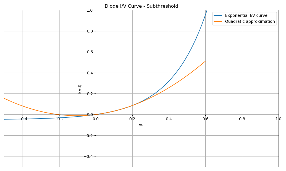
The real I/V curve is still exponential, of course, but below 0.3V, it can be approximated very well with a quadratic curve. In this case, the exponential curve has been aproximated by \(I(V_d)=1.055V_d^2+0.219x\).
The quadratic behavior can be explained with a little bit of high school calculus. The Taylor series of an exponential function is:
\[e^x = 1 + x + \frac{x^2}{2!} + \frac{x^3}{3!} + \frac{x^4}{4!} + \frac{x^5}{5!} + \cdots\]For small values of \(x\), we can approximate the series above as follows:
\[e^x \approx 1 + x + \frac{x^2}{2}\]If we substitute \(x\) by \(\frac{V_d}{nV_T}\), then for small \(V_d\), the I/V curve now looks like this:
\[I(V_d) \approx I_S[(\frac{V_d}{nV_T}) + \frac{1}{2}(\frac{V_d}{nV_T})^2]\]That’s nice, but there’s still a linear and a power-of-two term. Are there cases where there’s just the power-of-two term left? There is!
Here’s what happens when the voltage across the diode is a sine wave with amplitude \(V_p\) and frequency \(f\): \(V_d = V_p\cos(2\pi f)\).
\[\begin{align*} I(V_d) &\approx I_S[(\frac{V_d}{nV_T}) + \frac{1}{2}(\frac{V_d}{nV_T})^2] \\ &\approx I_S\frac{V_p}{nV_T} \cos(2\pi f) + \frac{I_S}{2}[\frac{V_p}{nV_T}\cos(2\pi f)]^2 \\ &\approx I_S\frac{V_p}{nV_T} \cos(2\pi f) + \frac{I_S}{2}(\frac{V_p}{nV_T})^2\frac{1 + \cos(2 \cdot 2\pi f)}{2} \\ &\approx I_S\frac{V_p}{nV_T} \cos(2\pi f) + \frac{I_S}{4}(\frac{V_p}{nV_T})^2[1 + \cos(4\pi f)]\\ \end{align*}\]If we apply a low pass filter with a cutoff well below frequency \(f\), then the equation above reduces to:
\[I_{dc} = \frac{I_S}{4}[\frac{V_p}{nV_T}]^2\]Under the right conditions, the current through the diode is proportional to the power of two of the amplitude of the sine wave.
The quadratic approximation is not only heavily dependent on temperature, but also on the silicon. You can buy 2 diodes of the same type, and keep them at the same temperature, yet their I/V curves might still be shifted quite a bit from each other.
That’s less of a problem when the diode is operating in the region above the threshold, the resistance is too low to matter, but subthreshold, the resistance will be much higher, often higher than the resistance that’s in series with the diode.
We’ll soon get back to square law behavior.
The HP 423A Crystal Detector
The HP 423A is a low-barrier Schottky diode detector. First mentioned in a November 1963 edition of HP Journal, the HP 423A is old. The Keysight product page predictably lists it as obsolete, but they still sell a 423B.
Going through the specs, there are a couple of differences: the 423A only sustains an input power of 100mW (20dBm/6.3Vpp) vs 200mW (23dBm/8.9Vpp) for the B version. There are are also differences in output impedance, frequency response flatness, sensitivity levels, noise levels and so forth. But the supported frequency range is the same, from 10MHz to 12GHz.
For my basic use, the input power limits are important, exceeding them of a prolonged time will damage the device, but the other characteristics don’t matter a whole lot since I barely know what they mean to begin with.
100mW/20dBm of power is pretty high for test and measurement equipment, and well above the the maximum 15dBm output of my sweep and signal generator.
Despite their differences, the 423B datasheet explains the basics about how they work and some of its applications.
In their words:
These general purpose components are widely used for CW and pulsed power detection, leveling of sweepers, and frequency response testing of other microwave components. These detectors do not require a dc bias and can be used with common oscilloscopes, thus their simplicity of operation and excellent broadband performance make them useful measurement accessories.
If they’re so useful for measurements, then let’s just cut to the chase and do exactly that.
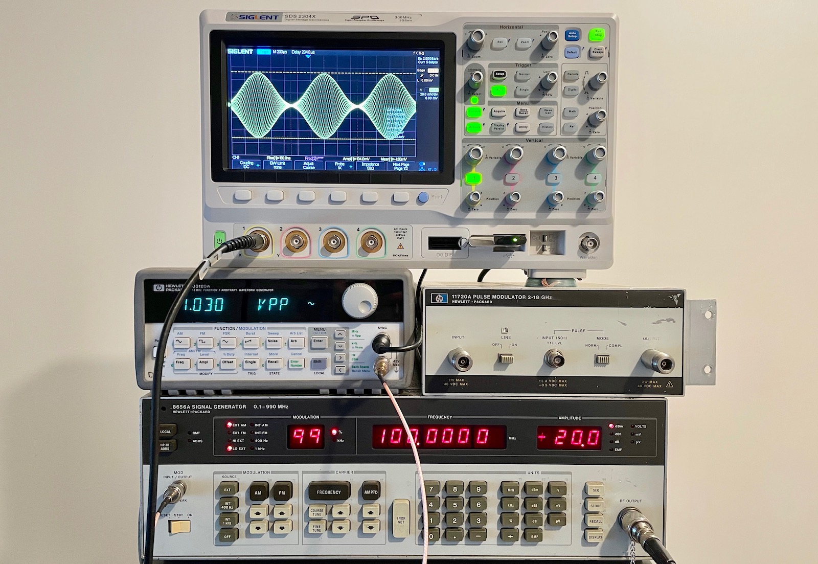
The Crystal Detector in Action
The setup below has the 8656A RF signal generator configured to generate a 100MHz carrier waveform at a -20dBm power level. It’s set to AM mode and expects an external signal on its modulation input. A 33120A signal generator is sending out 1 kHz 1Vpp sine wave to that input.
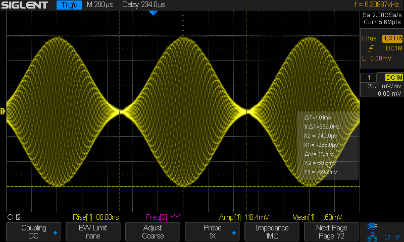
The sample rate of scope is way below the 100MHz carrier, but it shows the outline of a 1kHz envelop of the AM signal very well:
 Click to enlarge
We now connect the crystal detector to the output of the RF generator.
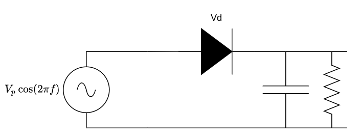
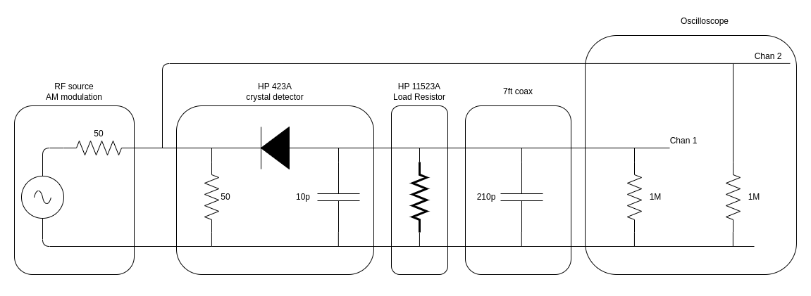
The setup has the following equivalent schematic:
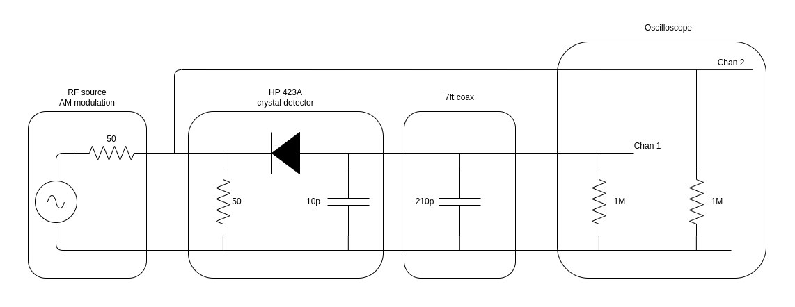
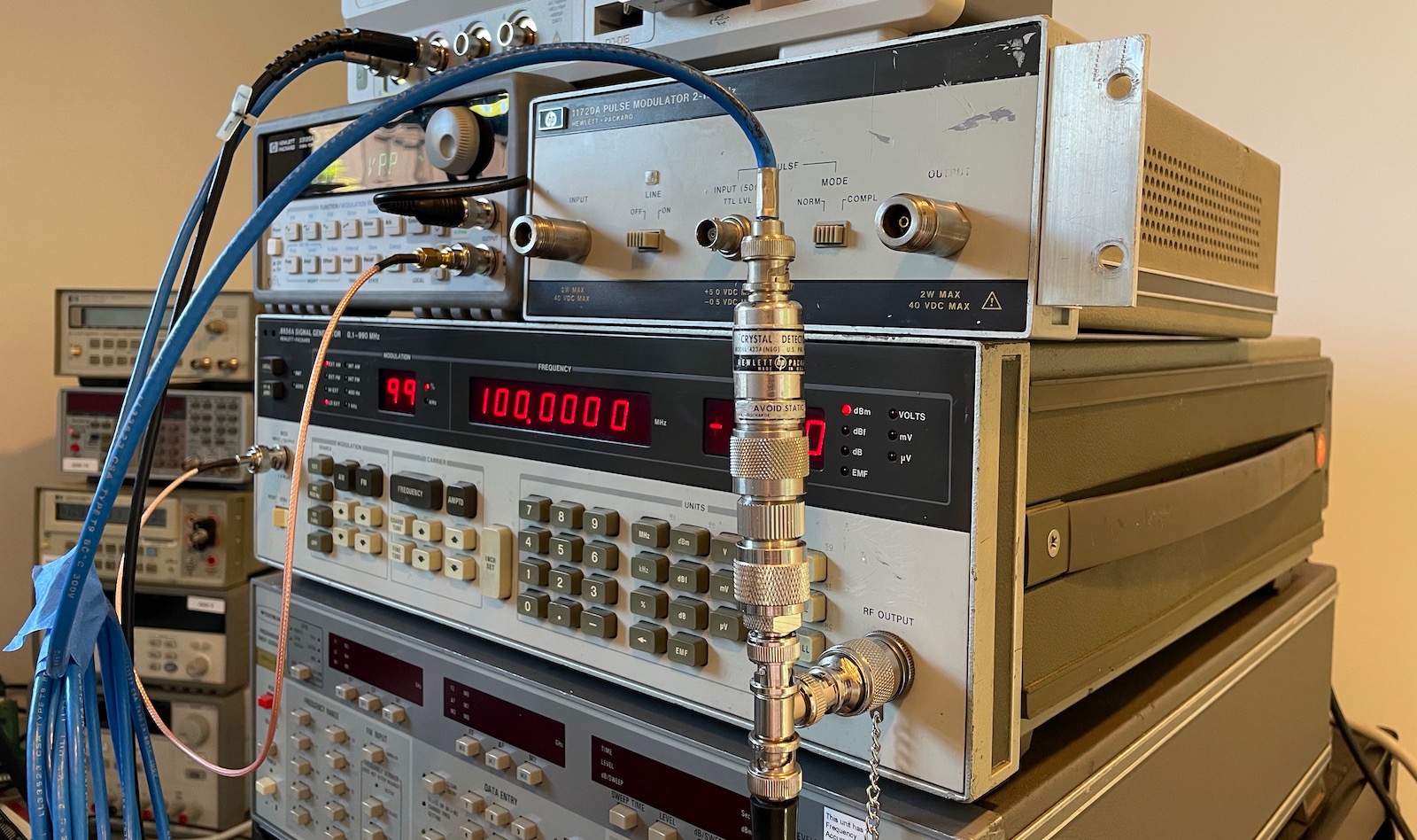
Since the crystal detector has a 50Ω input impedance, the input impedance of channel 2 of the scope is set to 1MΩ to avoid having two 50Ω loads on the RF source. The HP 423A operating manual lists a detector output impedance of <15kΩ, shunted by 10pF. We’ll get back to that 15kΩ later, but the capacitor in the schematic above is the one of 10pF.
In addition to the capacitor inside the detector itself, there’s also the capacitance of the coax cable between the detector and the scope. The one that I’m using is 7ft long. At ~30pF/ft, the cable alone adds another 210pF, which dwarfs the detector capacitance. Not for nothing, the operation manual has following:
when using the crystal detector with an oscilloscope, and the waveshapes to be observed have rise times of less than 5us, the coaxial cable connecting to the oscilloscope and detector should be as short as possible and shunted with a resistor.
The reason they’re talking about the rise time is that the cable capacitance will be part of an RC low-pass filter that dulls the edges on an RF pulse at the input. This is important if you want to use a crystal detector to check the slope of pulses that come out of a pulse modulator, like the HP 11720A that I wrote about earlier.
Channel 1 of the scope, connected to the output of the detector, is also set to 1MΩ to avoid loading the output too much.
The diode of the detector is in ‘opposite’ direction. This doesn’t fundamentally change the operation, it will pass through the negative part of the incoming signal. This is the default configuration for many of these kind of dectectors, but HP/Keysight, also sell an option with the diode oriented the other way around.
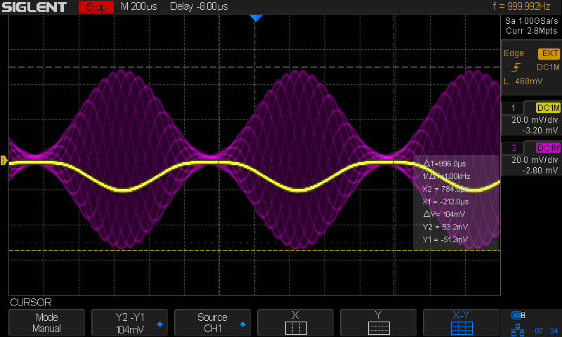
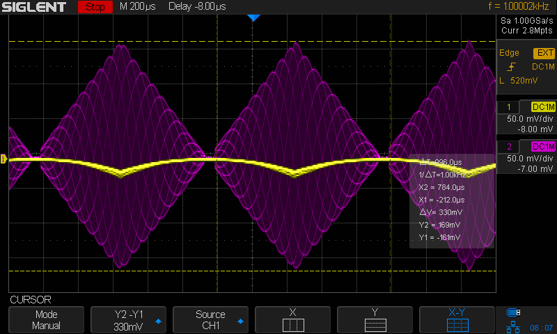
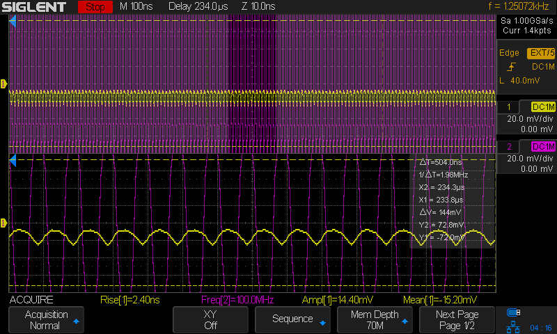
Let’s now see the result on the scope. The purple waveform is now the direct output of the signal generator, and the yellow is the one from the crystal detector.
 Click to enlarge
As expected, the output of the detector is negative, a consequence of the diode pointing to the left.
The detected signal looks a bit like but is not quite a sine wave, and the smaller the envelope of the original signal, the less the detector output seems to follow the envelope.
This is also expected. The oscilloscope cursor shows that an RF signal peak of ±53mV. The diode of the detector is operating in the square law region!
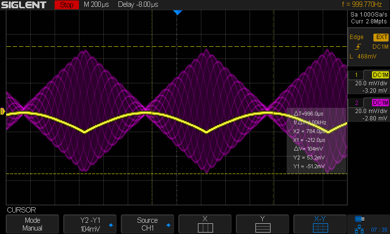
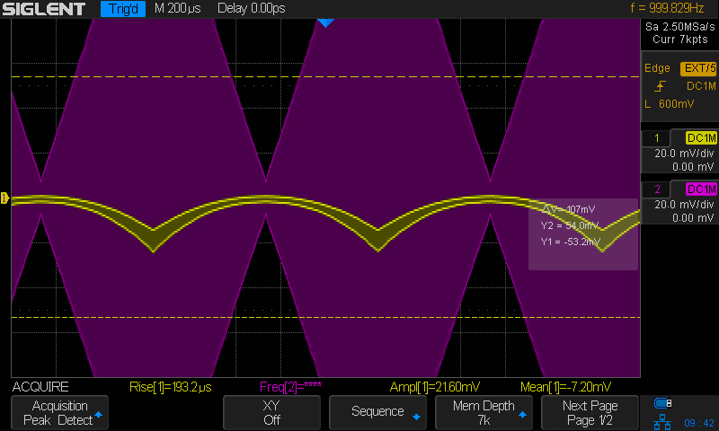
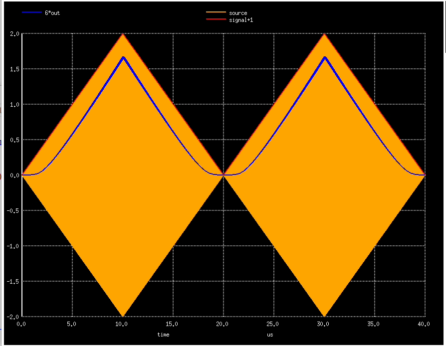
This becomes even clearer when we modulate the RF signal with a triangle waveform instead of a sine wave: the detector output is now a parabola:
In the current setup, the only resistor at the output of the detector is the 1MΩ load of the oscilloscope. For low power Schottky diodes, the square law region of a detector in such a configuration runs roughly until -20dBm/63mVpp, which is how I have configured output level of the signal generator.
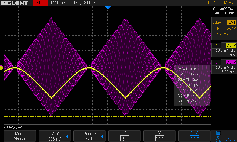
When I increase the output level of the signal generator to -10dBm/0.2Vpp, the output still looks curved close for the small signals, but it definitely looks more linear for higher values.
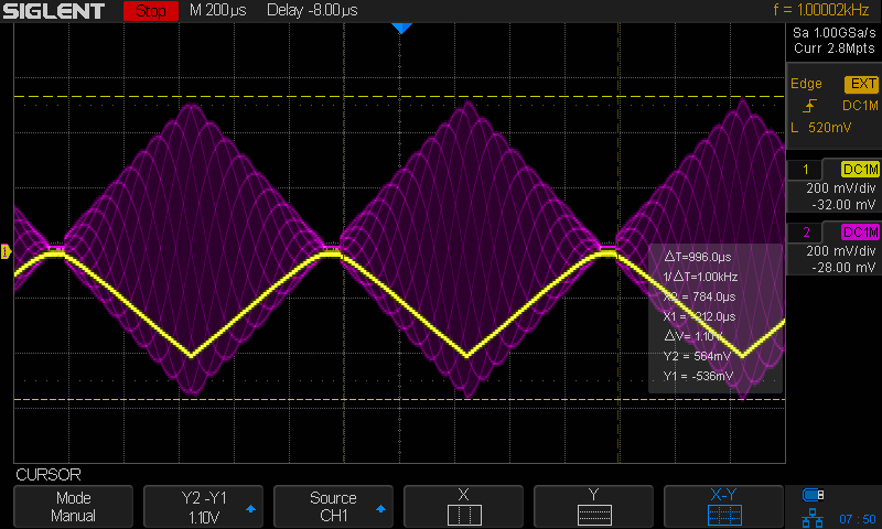
Raising the output by 10dBm once more to 0dBm/0.63Vpp, and there’s very little left of quadratic behavior.
If -20dBm corresponds to 63mVpp, and -10dBm to 0.2Vpp, then why does the cursor on the scope shots show a ΔV of 104mV and 330mV? It’s because the dBm to Vpp formula assumes a fixed amplitude sine wave. In our case, the signal is amplitude modulated, so the peak signal excursion is larger to compensate for times where the amplitude is lower.
Playing with the Detector Load
Without a load resistor, or better, with a very weak load resistor of 1MΩ, the square law region of the detector goes from around -50dBm to around -20dBm. There’s nothing much we can do about the lower bound of -50dBm: below that you’re essentially measuring noise. But it is possible to increase the square law region upwards to -10dBm, by adding a load resistor at the output of the detector.
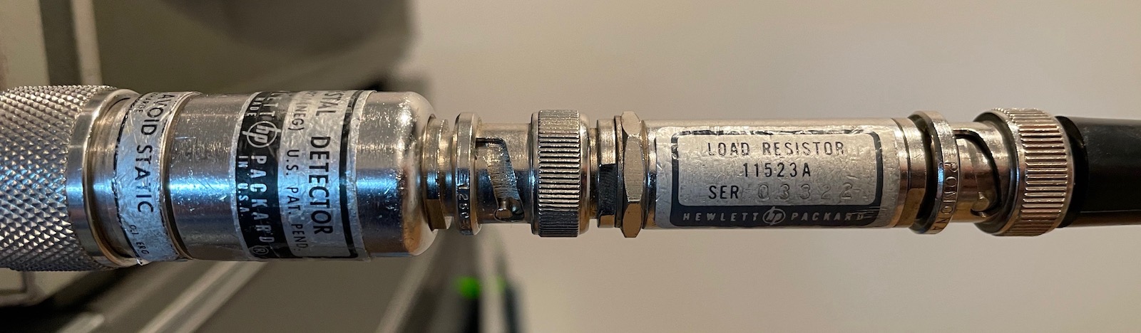
HP 11523A is exactly that: “a matched load resistor for optimimum square characteristics”. I’ve measured the resistance to be 562Ω. I don’t know which criterium is used to determine value of the matched resistor, but I’ll give it a try further below.
Here’s what happens with our signal for the -10dBm case:
The detector output (yellow) is definitely quadratic again, but the amplitude of the detector output is much smaller as well. And the yellow line also has a weird kind of fuzziness.
Smaller Output Voltage
The reason for the smaller detector output is simple: reducing the value of load resistor has shifted the voltage divider so that the diode has a larger share of the total input voltage.
\[V_{out} \propto \frac{R_{load}}{R_{load}+R_{diode}}\]\(R_{diode}\) is a moving target and depends on the voltage \(V_d\), but we’ve reduced \(R_{load}\) from 1MΩ to 562Ω, a factor of more than 2000. The voltage ratio has definitely shifted toward the diode.
Output Signal Fuziness
If we change the vertical scale of the scope and switch the scope to peak detect mode, we can have a better look at the output signal:
It’s clear that there’s a lot of variation on the detector signal output.
We can see what happen when we change the timebase of the scope from 200us, perfect to observe the 1kHz amplitude modulated envelope, to 5ns, which is needed to observe the 100MHz RF carrier:
By reducing the load from 1MΩ to 562Ω, we have dramatically changed the time constant of the RC circuit that is formed by the capacitor inside the detector, only 10pF, the capacitance of the coax cable that is connected to the detector, ~210pF, and the load resistor.
With the 1MΩ load, the time constant is around \(220\times10^{-12} \cdot 10^{6} = 220us\), way above the 10ns clock period of the 100MHz signal. With the 562Ω load, that number reduces to \(220\times10^{-12} \cdot 562 = 123ns\). That’s still well above 10ns, but keep in mind that the time constant is the time needed to discharge a capacitor by 63%.
In the waveform above, we’re nowhere close to that, and the capacitance is only a rough guess as well.
There are tradeoffs to be made when choosing a detector configuration:
- where do you want the square law region to end?
- what’s the frequency of the AM modulated signal?
- what’s the frequency of the RF signal
- how much ripple on the detected signal is acceptable?
Why Do We Want Square Law Behavior Anyway?
Square law behavior makes the detector react quadratically to the amplitude of an RF signal. In most signal processing systems, non-linear behavior is something you want to avoid at all cost, because it distorts the signal.
Yet it’s clear from the operating manual, and most other crystal detector literature, that square law behavior is often a feature.
That’s because crystal detectors are often used to measure the power of an RF signal, and \(P \sim V^2\). If we operate the detector in the square law region and measure its output, the voltage that we get is proportional to the power of the signal.
Note that I wrote ‘proportional’, not ‘equal’, because of the aforementioned issue with the square law formula of a diode: it’s heavily dependent on temperature and silicon.
Why Does the Load Resistor Shift the Square Law Region?
Here’s a thing that I didn’t get for the longest time: if the square law region of a crystal detector runs up to -20dBm with a 1MΩ load resistor, why does it shift upwards when you use a load resistor with a much lower value?
With a lower load resistor, the voltage across the diode will increase, not decrease, which means that you’ll much quicker reach the point where the diode I/V curve behaves quadratically?
I had to run a couple of ngspice simulations before I figured it out. First with a real AM signal, which matched my scope shots nicely.
But I soon switched to a diode-resistor configuration without amplitude modulated signal. It makes things much easier to understand.
When the source voltage is zero, the diode resistance will initially be very high (blocking), much higher than the load resistance, and the source voltage will be primarily over the diode.
As the source voltage increases, the resistance of the diode will decrease. Since the resistance of the load resistor stays constant, the voltage ratio will shift from diode to the resistor. Because the increase in source voltage only gets applied partially over the diode, the current through the diode won’t increase quadratically (square law), but less than that.
The extent by which this happens depends on the value of the load resistor.
When the load resistor is high, the resistance of the diode will quickly fall below the resistance of the diode. The current through the system won’t follow square law at all and will soon be entirely linear.
When the load resistor is low, it will take much longer before the resistance of the diode becomes lower than the load resistance. The lower the load resistance, the longer current through the diode will follow (more or less) the theoretical diode I/V curve.
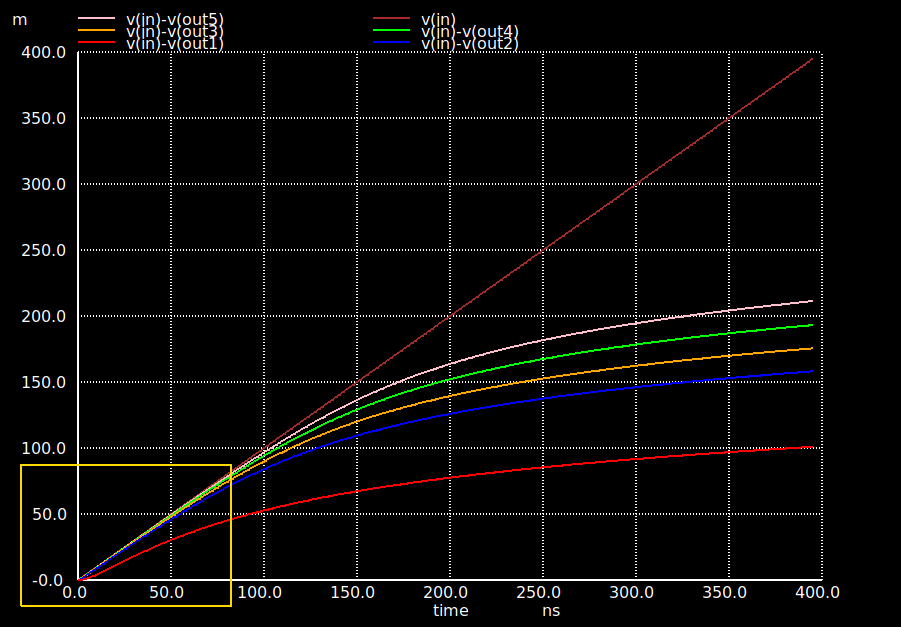
In the graph above, you can see the voltage over the diode for a linearly increasing \(V_{in}\). The top brown line is the source input. The bottom red line is for a 10kΩ load resistance. The lines above that are for decreasing load resistors: 2000Ω, 1000Ω, 500Ω and 250Ω.
For the 10k resistor, the voltage over the diode is already different than the input voltage right from the start, and as the input voltage increases, the voltage over the diode veers away in a non-linear way: the load resistor is getting an ever larger share of the input voltage. It takes a much longer time for this to happen with lower load resistor values.
Here you can see how that affects the output voltage:
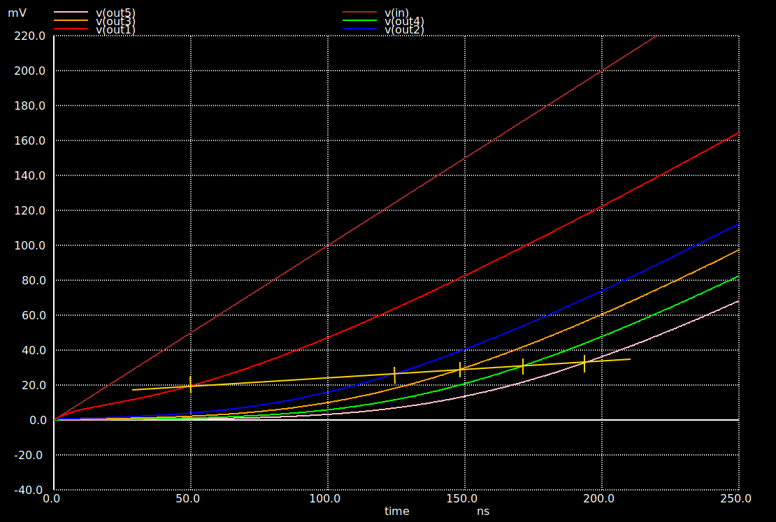
The lower the load resistor, the higher the \(V_{in}\) needs to be before output curves start to transition from clearly quadratic to mostly linear.
The markers along the yellow line show where that happens.
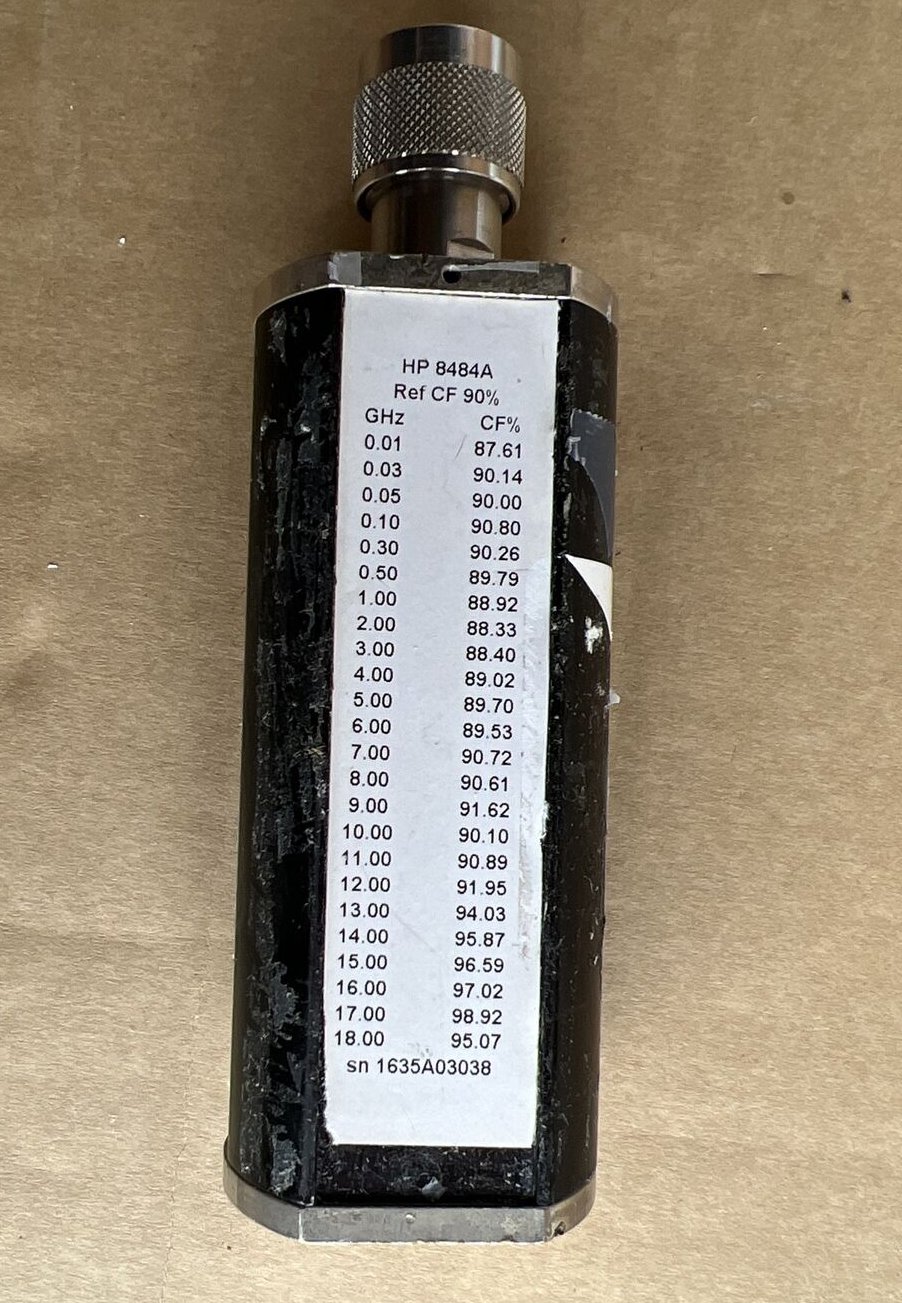
Power Measurement with Crystal Detectors
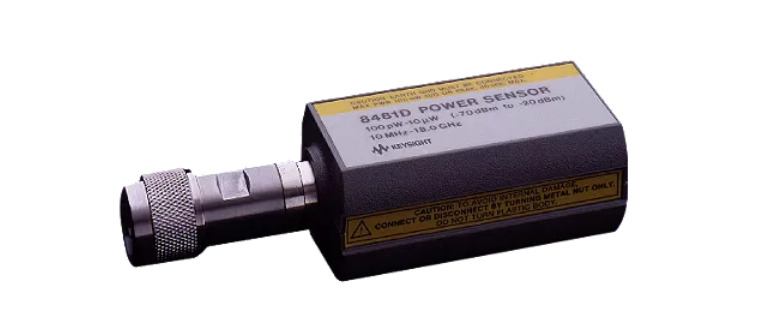
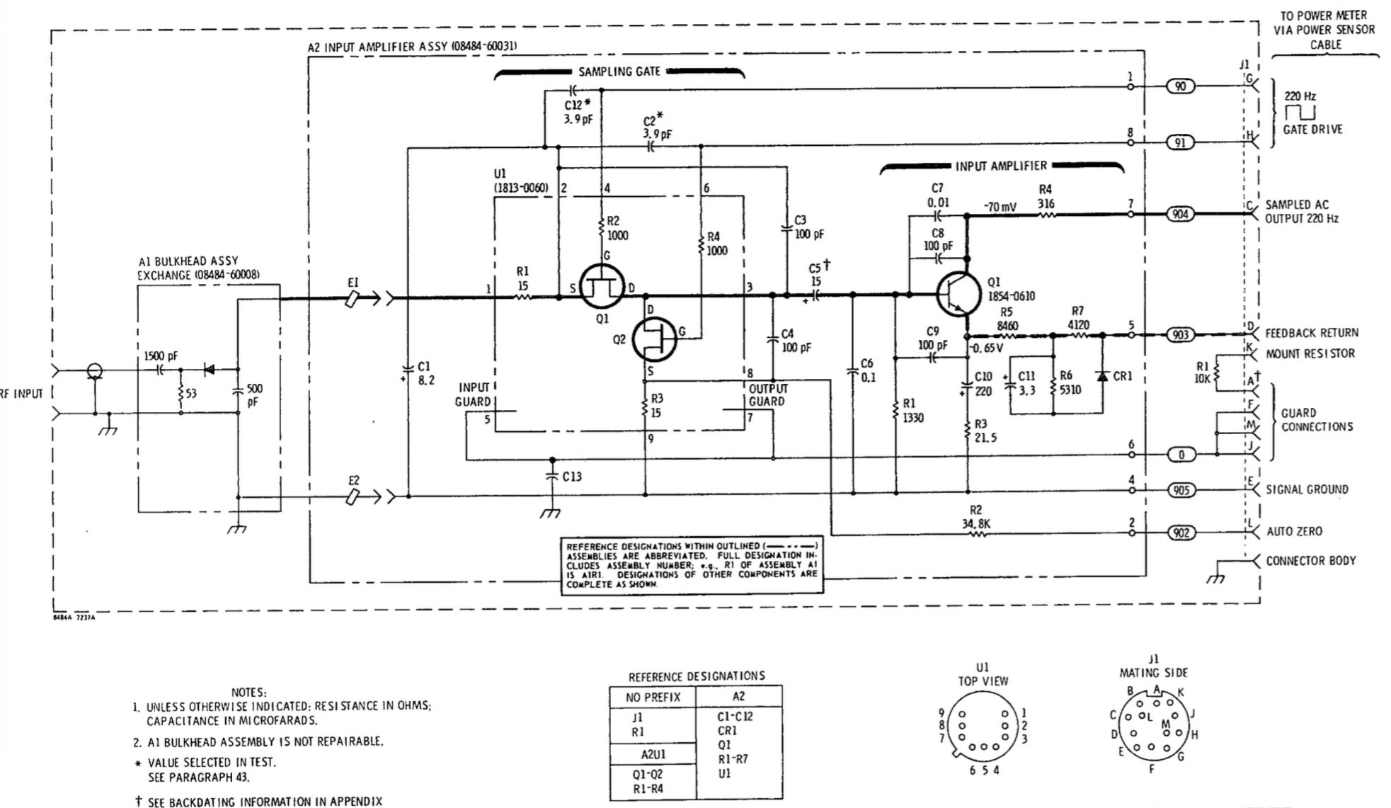
Now that we know that crystal detectors are the key sensor for a class of RF power meter, it’s time to have a look at one of them: the HP 8484A. Another oldie that’s now obsolete, but its specifications are close to the HP 8481D, which is still for sale, for a whopping $2724.
Here’s the schematic of the 8484A:
 (Click to enlarge)
Except for a DC-blocking capactor at the entrance, the schematic is exactly as one could expect: a 53Ω termination resistor2, the detection diode, and a capactor. The output of the detector goes to chopper circuit that samples the detector value at a rate of 220Hz.
How does a power meter with the temperature and silicon dependency of the detector diode?
The obvious option is to calibrate the sensor before making a measurement.
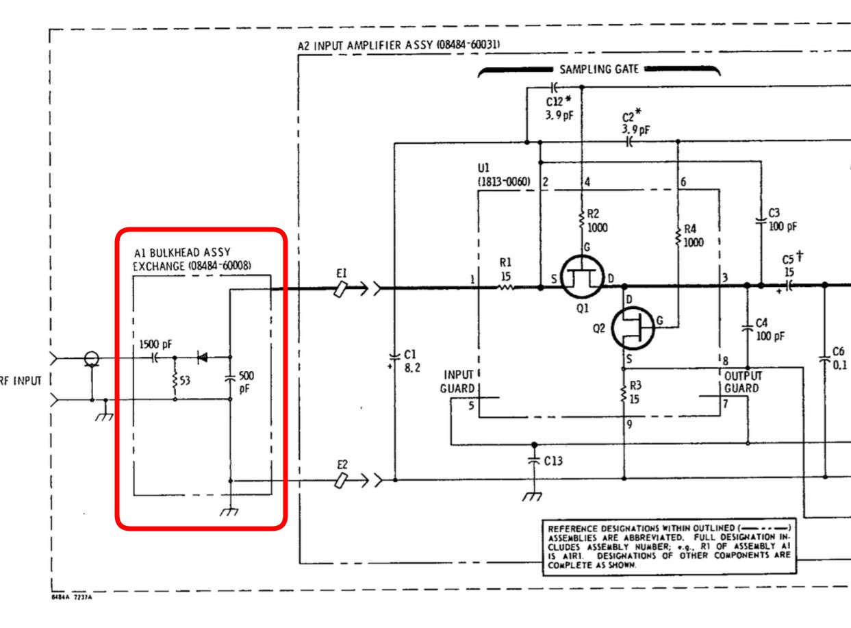
HP 8484A and 8481D sensors plug into an HP 438A power meter. These meters are much cheaper than the sensors. On a good day, you can find them for less than $100 on eBay, though mine is a John freebie.
In the center of the front panel, a 1mW/0dBm power reference is prominently featured, and there are also “ZERO”, “CAL ADJ”, and “CAL FACTOR” buttons. Before making a set of measurements, you first have to calibrate the power sensor before, otherwise the results will be all over the place.
But even calibration against the power reference is not enough. The reference output frequency is fixed at 50MHz, but the output of a crystal detector changes for different input frequencies, and the parameters of the diode I/V curve are silicon dependent. Each power sensor comes with their own calibration table. You have to manually enter the right calibration factor before measuring.
Keysight has a large arsenal of RF power sensors with different frequency and power ranges. The HP 8484A and 8481D sensors shall only be used for RF sources with a maximum power level of -20dBm. To calibrate those against a device like the HP 438A, you always need to use an HP provided reference attenuator.
I don’t have a power sensor yet for my HP 438A, but Daniel Tufvesson has been hard at work at building one himself.
References
Crystal Detector
- HP 423A and 8470A Crystal Detector - Operating and Service Manual
- HP Journal Nov, 1963 - A New Coaxial Crystal Detector with Extremely Flat Frequency Response
- Agilent 8473B/C Crystal Detector - Operating and Service Manual
Square Law
- HP RF & Microwave Measurement Symposium and Exhibition - Characteristics and Applications of Diode Detectors
- Agilent AN980 - Square Law and Linear Detection
- Square Law Detectors
- Diode Detector - Principle of Operation
Power Measurement & Power Leveling
- HP AN 64-1A - Fundamentals of RF and Microwave Power Measurements
- HP AN 218-5: Obtaining Leveled Pulse-Modulated Microwave Signals from the HP 8672A
- Infineon - RF and microwave power detection with Schottky diodes
- RF Diode Detector Measurement
- Diode detectors for RF measurement Part 1: Rectifier circuits, theory and calculation procedures.
- Analog Devices - Understanding, Operating, and Interfacing to Integrated Diode-Based RF Detectors
- DIY Power Sensor for HP 436A and 438A
AM Demodulation
Spice